


- News
15 March 2016
EFFECT Photonics samples its first optical system-on-chip product family
EFFECT Photonics b.v. – a spin off from the Technical University of Eindhoven (TU/e) in The Netherlands that develops optical components using indium phosphide (InP)-based multi-channel photonic integrated circuits (PICs) for mobile networks and data-centers – is launching its first product family based on its optical system-on-chip technology platform (which integrates all the active and passive components of a DWDM system within a single chip, without traditional gold box packaging). The launch is the culmination of 5 years work to bring the technology to market-readiness.
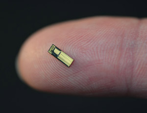 Picture: EFFECT Photonics' optical system-on-chip. .
EFFECT Photonics is aiming to address soaring demand for affordable bandwidth between data-centers and back from mobile cell towers by bringing dense wavelength division multiplexing technology to the edges of the network. By using high-integration system-on-chip technology, port density can be increased by over six times and operational expenses reduced by 40% compared with existing approaches, the firm reckons.
The product family includes transceivers for the transmission of 100Gbps over 80km targeting the lowest cost and power, together with high-density solutions containing many wavelengths for emerging WDM access markets in front-haul, back-haul and NG-PON2. Industry-standard sockets are supported including CFP and CFP2, so the products can be used in existing and future systems.
"We could see a bandwidth crunch coming at the edges of the network and knew that DWDM could be the answer, but it had to be done differently, so we developed a holistic solution from the ground up," says CEO James Regan. "We have completely re-thought how to tackle the issues of cost, power and density," he adds. "As well as integrating many optical functions into a single chip, we have reduced the cost and complexity of our packaging, resulting in a commercially viable solution. We are now at the sampling stage," Regan continues.
"100Gbps over 40-80km is a significant market opportunity that has no cost-effective solution today," comments Andrew Schmitt, founder & principal partner at market analyst firm Cignal AI. "This is the next battleground for 100G solutions."
EFFECT is showcasing its new product family in booth 2833 at the Optical Fiber Communication Conference & Exposition (OFC 2016) in Anaheim, CA, USA (20-24 March).


