


- News
9 March 2016
III-V field-effect transistor transconductance record
Massachusetts Institute of Technology in the USA has claimed record transconductance performance for a self-aligned planar indium gallium arsenide (InGaAs) quantum-well metal-oxide-semiconductor field-effect transistor (MOSFET) [Jianqiang Lin et al, IEEE Electron Device Letters, published online 19 February 2016].
The maximum transconductance of 3.45mS/μm at 0.5V drain bias was attributed to a re-designed access region with increased carrier concentration. The new design overcomes problems with source starvation and the consequent shift of the virtual source point into the access region, reducing gate control of channel conductivity.
The researchers comment that 3.45mS/μm is a record value among III-V FETs of any kind, including MOSFETs and high-electron-mobility transistors (HEMTs).
Funding for the research came from US Defense Threat Reduction Agency, US National Science Foundation Energy Efficient Electronics Science Center, Lam Research, Northrop Grumman and Singapore-MIT Alliance for Research and Technology Center. The research is aimed at future high-performance low-power CMOS electronics.
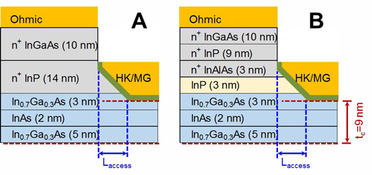
Figure 1: Simplified device cross-section schematic and respective heterostructures used. Layers labeled with n+ are silicon-doped 3x10¹⁹/cm3—4x1019/cm3, otherwise they are undoped.
The researchers produced two heterostructures with different n+-cap designs (Figure 1). In one, design A, the the n+-cap is directly in contact with the InGaAs channel layers. The other, design B, has an undoped indium phosphide (InP) spacer.
Design B with undoped spacer is similar to the structure used in MIT's previous transistor work. The researchers comment: "The elimination of the undoped InP spacer in design A results in a higher electron density in the InGaAs/InAs/InGaAs channel layer in the as-grown structure."
The heterostructures were fabricated into self-aligned transistors with 15nm access regions and 2.5nm hafnium dioxide high-k dielectric/metal gate (HK/MG) structure. The equivalent oxide thickness (EOT) was 0.5nm. The gate was recessed using a combination of dry etch and a self-limiting digital etch. The digital etch allows precision engineering of the transistor dimensions. The process can reach surface roughness values as low as 0.2nm root-mean-square.
Design A devices with 1μm gate length have achieved subthreshold swing values of 66.6mV/decade at 10mV drain bias. This matches the lowest subthreshold swing reported for any planar InGaAs MOSFET, according to the researchers. Devices with 70nm gate length achieved subthreshold swings of 150mV/decade and 115mV/decade for 0.5V and 0.05V drain, respectively.
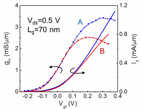
Figure 2: Transconductance (gm) versus over-gate overdrive with respect to threshold (Vgt = Vgs-Vt) and drain current (Id) transfer characteristics of 70nm MOSFETs A and B.
The 70nm MOSFET achieved a maximum transconductance of 3.45mS/μm at 0.5V drain (Figure 2). The team reports: "This represents an 11% improvement over the previous records in planar InGaAs MOSFETs and HEMTs, both at 3.1mS/μm." A comparison device using design B managed a peak transconductance of only 2.55mS/μm at the same bias.
http://ieeexplore.ieee.org/xpl/articleDetails.jsp?arnumber=7414406
The author Mike Cooke is a freelance technology journalist who has worked in the semiconductor and advanced technology sectors since 1997.


