


- News
11 March 2016
Indium gallium nitride barriers enhance LED power and efficiency
South China University of Technology has shown improved power and efficiency performance for indium gallium nitride (InGaN) light-emitting diodes (LEDs) with 1.2% indium-content multiple-quantum-well (MQW) barriers [Zhiting Lin et al, J. Phys. D: Appl. Phys., vol49, p115112, 2016].
The purpose of the research was to study the effect of indium in MQW barriers. Most commercial MQW designs use pure GaN barriers (i.e. 0% indium).
The epitaxial heterostructures were grown by metal-organic chemical vapor deposition (MOCVD) on 2-inch (0001) patterned sapphire (Figure 1). The undoped buffer layer was 4μm. The n-GaN contact was 3μm. The electron-blocking layer (EBL) and p-contact were 20nm and 150nm, respectively.
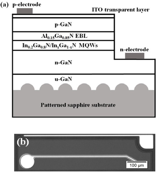
Figure 1: (a) Epitaxial structure of as-grown LEDs; (b) optical micrograph of chip.
The MQW region consisted of seven 3nm wells separated by 14nm barriers. The wells had 20% indium content. The variation in indium content in the barriers was achieved through changing the trimethyl-indium precursor flux. The indium content was evaluated using x-ray diffraction analysis.
Standard InGaN LED chips were fabricated with 250nm indium tin oxide (ITO) transparent conductor, and chromium/platinum/gold n- and p-electrodes. The chip dimensions were 750μmx220μm.
The highest light output power above 20mA injection current was achieved with 1.2%-In barriers (Figure 2) – at 70mA the increase in output power over pure GaN barriers was 15.4%. The light output decreased significantly when the indium content exceeded 2%.
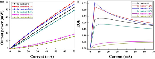
Figure 2: (a) Light output power versus current and (b) EQE versus current.
Although the 2.0%-In barrier gave the highest peak external quantum efficiency (EQE), the 1.2%-In barrier was better at reducing the droop effect at higher injection current. At 70mA, the 2.0%- and 1.2%-In barriers gave EQE values 3.3% and 10.3% better than for pure GaN barriers.
The researchers therefore consider 1.2% indium to be the optimal content for InGaN barriers. X-ray analysis suggested that problems with increased indium content included increasing roughness of the well/barrier interface and degraded crystal quality.
One cause of such problems could be the increased lattice mismatch between the barrier and the underlying GaN lattice constant. The thinner wells should be less affected by crystal quality degradation, despite the higher indium content. However, the reduced crystal quality of the barriers and the interface roughness do have their effect on the quality of subsequent well growth, inducing the creation of non-radiative recombination centers.
Photoluminescence analysis showed a slight reduction in intensity for 1.2%-In barriers, compared with pure GaN. As the indium content was increased beyond 1.2%, the photoluminescence decreased sharply.
The researchers used simulations to suggest that a positive effect of increasing indium content in the barriers was to increase carrier concentrations in the MQW structure. "We propose that the gain on carrier concentration and the crystalline quality degradation are a pair of opposite influential factors as the indium content of InGaN barriers increases," they write.
The calculations also suggest that the increase in indium increases the potential barrier for electrons while reducing that for holes.
InGaN LEDs MQW barriers InGaN MOCVD
http://dx.doi.org/10.1088/0022-3727/49/11/115112
The author Mike Cooke is a freelance technology journalist who has worked in the semiconductor and advanced technology sectors since 1997.


