


- News
14 March 2016
Direct growth of III-V quantum dot lasers on silicon substrate
Researchers in the UK have claimed the first demonstration of laser diodes grown directly on silicon that perform up to 75°C and 120°C under continuous wave (cw) and pulsed operation, respectively [Siming Chen et al, Nature Photonics, published online 7 March 2016].
Direct growth of laser structures on silicon could lead the way to lower-cost processing, and hence wider commercialization of silicon-based photonics integrated with CMOS electronics. Potential applications include communications, healthcare and energy systems.
Presently, combining laser diode technology with silicon involves tricky wafer bonding techniques. Better quality III-V direct growth on germanium (Ge) can be achieved either as a substrate or as an intermediate layer on silicon ('virtual substrate'). However, the presence of germanium can limit the range of accessible silicon electronic circuitry. Also, germanium absorbs the infrared light typically used in communications.
Direct growth of efficient III-V light-emitting semiconductor material on silicon has been hampered by reduced crystal quality due to lattice mismatches between the different crystal layers. The team from University College London, University of Sheffield, and Cardiff University used a number of techniques to reduce the effect of defects on the indium arsenide (InAs) QDs in gallium arsenide (GaAs) barrier material, which was the basis of the active light-emitting region in their devices.
The InAs/GaAs materials were grown by molecular beam epitaxy (MBE) on phosphorus-doped n-Si (100). The off-cut angle was 4° to the [011] plane to avoid anti-phase domain formation. A thin 6nm aluminium arsenide (AlAs) nucleation layer was deposited in a 350°C migration-enhanced process to suppress the three-dimensional growth mode.
Next, a GaAs buffer was grown in three steps: 30nm at 350°C, 170nm at 450°C, and 800nm at 590°C. This confined most defects to the first 200nm of growth, but a significant fraction escaped to give a 1x10⁹/cm2 threading dislocation (TD) density.
To improve material quality, a strained-layer superlattice (SLS) was grown as a dislocation filter. The superlattice consisted of four repeats of five pairs of 10nm/10nm In0.18Ga0.82As/GaAs separated by 300nm GaAs spacers.
The researchers comment: "The strain relaxation of the SLSs applies an in-plane force to the TDs, which enhances the lateral motion of TDs considerably, and hence increases the probability of annihilation."
In-situ thermal annealing in the MBE reactor was carried out on each of the four SLS sections by raising the temperature to 660°C for six minutes. This encouraged the TDs to move and annihilate.
The SLS dislocation filter was found to reduce TD density to the order of 105/cm2, "beyond the reliable measurement capability of cross-sectional TEM images," according to the researchers.
The ~20nm-diameter ~7nm-high QDs were grown in five dot-in-well (DWELL) layers with a density around 3x10¹⁰/cm2 and good uniformity. The well layers were 2nm and 6nm In0.15Ga0.85As before and after the dots. The DWELLs were separated by 50nm GaAs spacers. Photoluminscence measurements gave a peak around 1300nm wavelength (0.95eV) and 29meV full-width at half maximum.
The waveguide was 140nm. Cladding layers were 1.4μm n- and p-type Al0.4Ga0.6As. The p-contact was 300nm GaAs.
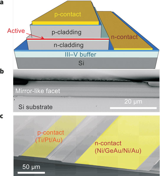
Figure 1: a, Schematic of layer structure of InAs/GaAs QD laser on silicon substrate. b, Cross-sectional SEM image of fabricated laser with as-cleaved facets, showing very good facet quality. c, Scanning electron microscope (SEM) overview of complete III–V laser on silicon.
Broad-area lasers (Figure 1) were fabricated with as-cleaved facets. The laser bars were mounted on gold-plated copper heat-sinks with low-melting-point indium-silver solder. Electrical connections were made with gold-wire bonding.
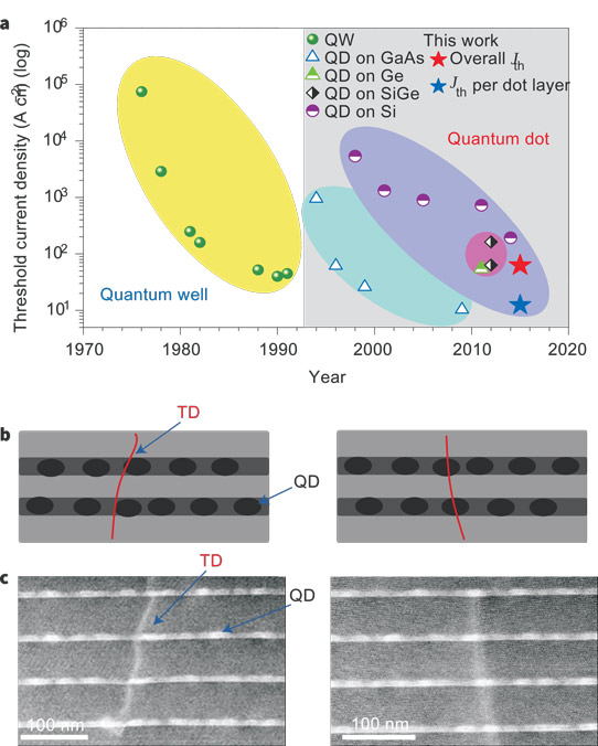
Figure 2: a, Development of low-dimensional heterostructure lasers, showing record threshold current densities. Red (upper) star indicates threshold value achieved in work reported here. Blue (lower) star is value normalized to single QD layer. b, Schematic of interaction between QDs and threading dislocations. c, Bright-field scanning transmission electron microscope (TEM) images showing potential interactions between threading dislocations and QDs.
The threshold current density (Jth, Figure 2) was 62.5A/cm2 (12.5A/cm2 per QD layer) under continuous wave (cw) operation. The researchers comment: "To the best of our knowledge, this value of Jth represents the lowest cw room-temperature Jth for any kind of laser on a silicon substrate to date and is comparable to the best-reported values for conventional QD lasers on a GaAs substrate."
The output power from both facets reached 105mW with 650A/cm2 injection without evidence of saturation.
With a view to high-temperature operation beyond 65°C needed for many silicon-based electronic operations, the researchers tested the device under cw and pulsed conditions. The cw lasing was maintained up to 75°C and pulsed lasing continued up to 120°C. The 75°C cw operation was limited by the current source. The researchers claim these as the first high-temperature performance figures for QD lasers grown directly on silicon.
A 3100-hour ageing test was also performed at 26°C and 210mA cw drive current (1.7x threshold). The output power degraded 29.7% over the test period with the greatest fall in performance (26.4%) occurring in the first 500 hours. The threshold trend was similar. The researchers extrapolate a mean time to failure (MTTF) of 100,158 hours, based on the time needed for a doubling of threshold current.
The team comments: "It should be noted that these data represent the worst-case results, because (1) the laser was operated epitaxial side up, (2) the laser was not hard soldered to a high-thermal-conductivity heat-sink, and (3) no facet coatings were used. Nevertheless, the estimated lifetime is much longer than the best reported extrapolated MTTF of 4,627 h for a p-doped InAs/GaAs QD laser grown on a Ge-on-Si 'virtual' substrate."
Quantum dot lasers GaAs Silicon substrate MBE
http://dx.doi.org/10.1038/nphoton.2016.21
The author Mike Cooke is a freelance technology journalist who has worked in the semiconductor and advanced technology sectors since 1997.


