


- News
14 March 2016
Noise and aluminium indium arsenide antimonide avalanche photodiodes
The universities of Virginia and of Texas in the USA have been developing avalanche photodiodes (APDs) based on aluminium indium arsenide antimonide (AlInAsSb) alloys. Two papers from the group detail the implementation of a staircase structure [Min Ren et al, Appl. Phys. Lett., vol108, p081101, 2016] and low-noise performance [Madison E. Woodson et al, Appl. Phys. Lett., vol108, p081102, 2016].
Staircase APDs were proposed in the early 1980s, but suitable semiconductor materials were not available at that time for the required bandgap engineering. The idea of the staircase steps is to reduce excess noise coming from electron multiplication in a way similar to dynode structures in photomultiplier tubes.
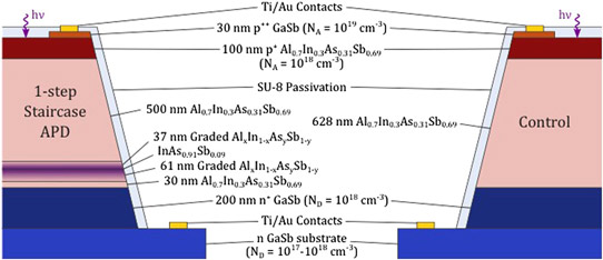
Figure 1: Schematic cross-sections of the 1-step AlInAsSb staircase APD (left) and control (right).
The structure of Ren et al (Figure 1) was grown by molecular beam epitaxy (MBE) on n-type gallium antimonide (n-GaSb) (001) substrates at 480°C. The alloying was achieved with a digital technique where the sources were shuttered in sequences that produced stable binaries of AlSb, AlAs, AlSb, InSb, InAs, and Sb.
The multiplication was achieved at the narrow-bandgap InAsSb (~0.25eV) step. The AlInAsSb injector region had a much wider bandgap (~1.16eV). The conduction band discontinuity was around 0.6eV.
The researchers comment that the threshold for impact ionization in narrow-bandgap materials is typically around 1.5x the bandgap. Since the conduction band drops 0.6eV from the injector, the electrons entering the step have more than 2x the bandgap energy of 0.25eV.
"This is sufficient to provide a high probability of impact ionization at the bandgap discontinuity," the researchers point out.
The step was sandwiched between digitally graded material that was designed to flatten the band edges in the graded layers to form a staircase-condition band structure at high bias.
The APDs were fabricated with circular mesas, SU-8 photoresist passivation, and titanium/gold contacts.
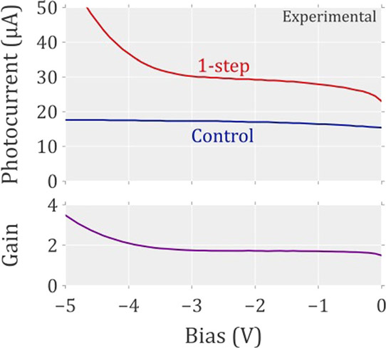
Figure 2: Enhancement of photocurrent from 50μm-diameter 1-step staircase APD over control at reverse biases up to 5V under 543nm wavelength.
The multiplication gain for 543nm wavelengths was found to be around 1.8 in the reverse-bias range 1V-4V (Figure 2). The measured gain is close to the 2x achieved in theory and Monte Carlo simulations.
The gain remains constant in the temperature range 80K-300K. Without composition grading between the InAsSb and AlInAsSb layers, the gain was reduced to about 1.6. The researchers suggest that the reduction could be due to the electrons losing energy at the abrupt interface. Varying the input wavelength up to around 950nm did not change the gain, although the response increased due to absorption in the InAsSb. The constancy rules out enhanced absorption, and confirms impact ionization as the source of the observed gain, according to the researchers.
Generally, noise scales as the square of the gain, suggesting an increase of ~3.2x for the graded APD. The measured noise was 2x-2.2x. "While fortuitous, this unexpectedly low noise will be the subject of future study," the researchers comment. They point out that similar noise suppression has been seen before in impact-ionization engineered heterojunction APDs.
The researchers believe their research could lead to separate absorption, charge and multiplication (SACM) AlInAsSb staircase APDs with cutoff wavelengths ranging throughout the short-wave and mid-wave infrared bands. Potential applications include night vision, thermal imaging, and free-space telecommunications. Multi-step devices should lead to higher gain.
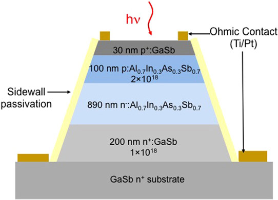
Figure 3: Cross-sectional schematic of low-noise APD.
Woodson et al used solid-source MBE on tellurium-doped n-GaSb to produce the structure for low-noise AlInAsSb APDs using digital alloying with 3nm period and an AlSb, AlAs, AlSb, InSb, InAs, Sb shutter sequence (Figure 3). Circular mesa APDs with SU-8 passivation were produced.
The resulting APDs had low excess noise performance (Figure 4), indicating extremely low k-factors – the ratio of hole to electron ionization probabilities. The behavior was consistent with a k-factor for the 30μm-diameter device of 0.015, comparable with silicon (~0.04). The excess noise factor from increasing gain was thus comparable to silicon devices. Indium phosphide (InP) APDs usually have k-factors in the range 0.45-0.52. The peak quantum efficiency of the AlInAsSb APD was 68% at 735nm.
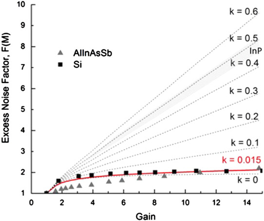
Figure 4: Excess noise factor versus gain for AlInAsSb and Si APDs. Solid lines are plots of excess noise factor using local field model for k values from 0 to 0.5. Lightly shaded region with k of more than 0.45 indicates typical InP APD performance.
Unlike silicon, AlInAsSb has a direct bandgap, which suggests that APDs based on the technology could achieve high bandwidths due to a shorter absorption length. Also, changing the composition of the material could lead to devices sensitive across the visible and near-infrared wavelength ranges. In particular, the 1μm to 12μm wavelength cut-off range is mentioned in the paper. A 1μm cut-off device would be sensitive to sub-micron wavelengths, such as visible light. Possible applications include optical communications, imaging, and single-photon detection.
http://dx.doi.org/10.1063/1.4942370
http://dx.doi.org/10.1063/1.4942372
The author Mike Cooke is a freelance technology journalist who has worked in the semiconductor and advanced technology sectors since 1997.


