


- News
11 May 2016
Integrating silicon photonics and III-V photodetectors in micro-spectrometer
Researchers based in Belgium, The Netherlands, the UK and France have realized heterogeneous integration of an indium arsenide antimonide (InAs0.91Sb0.09) photodiode array on a silicon-on-insulator (SOI) spectrometer for wavelengths as long as 3.8μm [M. Muneeb et al, Optics Express, vol24, p9465, 2016]. The team from Ghent University/imec, Eindhoven University of Technology, University of Southampton, and Université de Montpellier report: "To our knowledge this is the longest-wavelength integrated spectrometer operating in the important wavelength window for spectroscopy of organic compounds."
The researchers believe that such heterogeneous integration could also be applied to broadband light sources on-chip for fully integrated spectroscopic sensing systems.
The 3.8μm-wavelength mid-infrared region is important for spectral analysis of carboxylic acids. Shorter wavelengths of 3.3-3.5μm could cover hydrocarbons. Integration of the components required for such analysis on a single chip could lead to reduced costs and size for spectroscopic systems.
The arrayed waveguide grating (AWG) structure was built using silicon-on-insulator technology. The SOI wafer structure had 380nm of silicon on 2μm of buried silicon dioxide. The silicon layer was 220nm crystalline and 160nm polycrystalline. The waveguides were produced by etching 160nm and cladding with silicon dioxide.
The waveguides were designed for transverse electric (TE)-mode light with a center wavelength of 3.8μm. The array consisted of six channels spaced 9.6nm apart. The input and output ports consisted of grating couplers created through etching down 230nm. The researchers comment: "For the integration of the photodiodes we chose a grating-based coupling scheme because it is more fabrication tolerant as compared to other schemes like butt coupling or evanescent coupling." Grating couplers were also used for the input from optical fibers.
The upward angle for the light into the integrated III-V photodiode (Figure 1) was optimized through simulations varying the thickness of the top cladding of silicon dioxide and DVS-BCB cyclobutene polymer used as bonding agent.
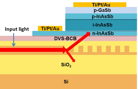
Figure 1: Schematic of grating-based coupling scheme.
The researchers used imec's CMOS pilot line to create the AWG structures. The top cladding silicon dioxide was 800nm, achieved through deposition and planarization. The smooth top cladding improves the photodiode bonding uniformity; reduces overlap between the waveguide mode and the bonding material that absorbs ~3μm light; and protects the underlying waveguide structure during photodiode fabrication.
The epitaxial material for the photodiode was grown on n-type gallium antimonide (GaSb) wafers using molecular beam epitaxy (MBE). The growth sequence consisted of 550°C deoxidation, 500°C GaSb buffer, 450°C 0.5μm InAs0.91Sb0.09 etch stop, 50nm p-GaSb/50nm p-InAs0.91Sb0.09 contact, 1μm unintentionally doped InAs0.91Sb0.09 absorber, and a 250nm n-InAs0.91Sb0.09 contact.
The III-V material was flipped and bonded to the AWG wafer using 300nm DVS-BCB. The 200μm GaSb growth substrate was lapped down to about 75μm before wet etching the remainder down to the etch-stop layer. The etch-stop layer was itself removed in another wet etch.
Further fabrication consisted of wet etching 30μmx45μm mesas aligned with the grating couplers, deposition of metal contacts, and DVS-BCB passivation of the photodiodes. The AWG region covered an area of 1.1mmx0.78mm. The total spectrometer area was 1.2mm2 (Figure 2).
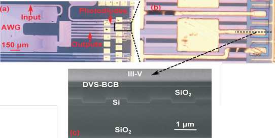
Figure 2: (a) Microscopic image of complete fabricated device, (b) close-up of single heterogeneously integrated photodiode and (c) scanning electron microscope (SEM) cross-section of photodiode.
The DVS-BCB passivation was found to be needed to create rectifying behavior in the photodiode by suppressing sidewall leakage currents. Even with passivation, the dark current was rather high: 600μA at -50mV and 170μA at -10mV. The researchers attributed 136μA to the photodiode and 34μA to sidewall leakage for the -10mV reverse-bias dark current.
The researchers point out that a homogeneous InAs0.91Sb0.09 structure is used for the p-i-n diode. High-bandgap barriers could reduce the bulk leakage and better passivation could be used to further reduce sidewall leaking.
The six channels covered wavelengths separated by about 10nm between 3740 and 3800nm. The crosstalk suppression was 16dB, which was worse than the 20dB of a passive system developed and reported by the group in 2013. The researchers attributed this to increased phase noise in the arrayed waveguide grating due to processing of the photodetectors.
The system responsivity ratio of photocurrent/optical power in the fiber was 1.1mA/W. The fiber-to-chip coupling efficiency was estimated to be -20dB. The AWG insertion loss is given as 3dB and the waveguide losses as 5dB/cm. The researchers therefore estimate the on-chip photodiode response to be 0.3A/W, corresponding to a quantum efficiency of about 10%. The quantum efficiency matches expectations from the simulations.
InAsSb Photodiode array on a SOI spectrometer Silicon photonics Photodetectors MBE
http://dx.doi.org/10.1364/OE.24.009465
The author Mike Cooke is a freelance technology journalist who has worked in the semiconductor and advanced technology sectors since 1997.


