


- News
4 May 2016
Quantum well/barrier intermixing blue-shift of indium gallium phosphide
King Abdullah University of Science & Technology (KAUST) in Saudi Arabia has developed a quantum well intermixing (QWI) technique to blue-shift indium gallium phosphide (InGaP) quantum well bandgaps to give 628nm red, 602nm orange and 585nm yellow electroluminescence [A. A. Al-Jabr et al, J. Appl. Phys., vol119, p135703, 2016]. The researchers see potential application in solid-state lighting, photodynamic therapy (PDT), medicine, and visible light communication.
The team reports: "A maximum blue-shift of 75nm (250meV) is achieved, which is the highest ever reported in this material system." The aim is to bridge the gap for high-efficiency light-emitting devices in the green-yellow-orange part of the visible spectrum between III-nitride (blue-violet) and III-phosphide (red) semiconductors.
Although the structure is designed as for a single QW (SQW) laser diode (LD), the researchers do not at this stage quote any laser characteristics such as current thresholds. "Our results show that this new QWI method technique may pave the way for the realization of high-efficiency orange and yellow light-emitting devices based on the InGaP/InAlGaP material system," they write.
The technique involves introducing strain into indium aluminium gallium phosphide (InAlGaP) heterostructures on gallium arsenide (GaAs) by depositing a thick layer of silicon dioxide (SiO2) and then applying a variety of thermal annealing processes.
The researchers believe the blue-shift is associated with the high strain arising from the thermal expansion mismatch between the silicon dioxide layer and the underlying semiconductor material.
The researchers explain: "During annealing, the mismatch in expansion at the interface of the dielectric and semiconductor induces high compressive strain, whereas the QW is under tensile strain. The opposite strains applied on the barriers create point defects at (1) the interface of the dielectric and the laser structure and (2) the interface of the barrier and the QW... These point defects, with energy given to the atoms by heat, facilitate the inter-diffusion of (group III) atoms between the QW and the barrier."
The researchers believe that the effect of the intermix is to increase the bandgap by the incorporation of Al in the InGaP and to alter the shape of the quantum well. The Al incorporation also reduces the strain of the QW, which also has a blue-shifting effect. The change in shape of the QW, making it effectively thicker, could subtract a small red-shift, but the total effect is to increase the bandgap over the as-grown material.
The waveguide properties are also affected by the intermixing between the InAlGaP barriers and InGaP QW. In particular, the defects will increase optical losses, leading to less efficient devices. Further problems are expected from the shift to yellow where optical losses in GaAs are higher.
High-Al-content InAlGaP layers grown directly by metal-organic chemical vapor deposition (MOCVD) or molecular beam epitaxy (MBE) tend to suffer from the presence of oxygen-related defects. The QW intermix technique is aimed at reducing or even eliminating such defects in the active QW layer.
The light-emitting structure consisted of a single InGaP quantum well in InAlGaP barrier/waveguide grown by MOCVD on 10°-offcut GaAs (Figure 1). The cladding layers were InAlP. The p-contact layers consisted of InGaP for injection barrier reduction and p-GaAs. The as-grown structure had peak room-temperature photoluminescence at 635nm±3nm.
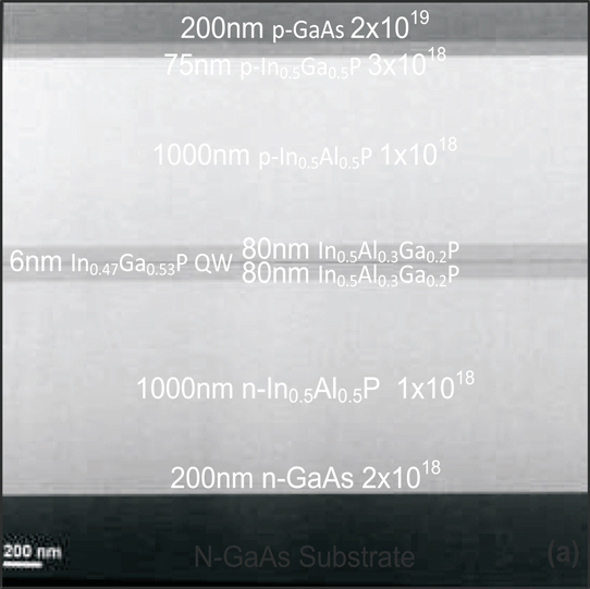
Figure 1: Dark-field (002) cross-sectional transmission electron microscope (TEM) image of InGaP/InAlGaP laser structure with a single QW.
The laser diode wafer was cleaved into approximate 2mm x 2mm pieces. These samples were coated with 1μm of silicon dioxide through plasma-enhanced chemical vapor deposition (PECVD) and annealed using a rapid thermal process.
The temperature and time of the rapid thermal anneal (RTA) was optimized to maintain strong photoluminescence intensity, narrow full width at half maximum (FWHM), and good surface morphology.
The desired blue-shift was found to occur at temperatures higher than 900°C for a 120 second anneal processes. Between 900°C and 950°C the rate of shift was around 1meV/°C. Above 950°C, the rate increased to around 3meV/°C. At 1000°C, the blue-shift was more than 60nm (200meV). Photoluminescence and surface morphology quality was maintained at temperatures up to 975°C.
Varying the anneal duration at 950°C also affected the blue-shift with an almost linear relation at a rate of 0.67meV/second, starting from about 45 seconds. Beyond 180 seconds the photoluminescence intensity decreased and the FWHM increased, indicating a reduction in quality. At 240 seconds, the peak wavelength shifted by 45nm (~140meV) to 595nm.
The problem of material quality deterioration was ameliorated by a cyclic process of a number of anneals at shorter intervals. The researchers considered the optimum step to consist of annealing at 950°C for 30 seconds. The researchers comment: "With this process, we were able to blue-shift the peak emission from red (640nm) to yellow (565nm) (250meV) with a number of cycles of annealing, which is the largest blue-shift reported for this material system."
Samples annealed for 2, 5 and 9 cycles had peak wavelengths at 620nm (red), 595nm (orange) and 575nm (yellow), respectively.
Devices for electroluminescence studies were fabricated by removing the capping dielectric and depositing front and back contacts. The electroluminescence peaks (Figure 2) were red-shifted between 5nm and 10nm due to self-heating effects from the broad-area current pumping.
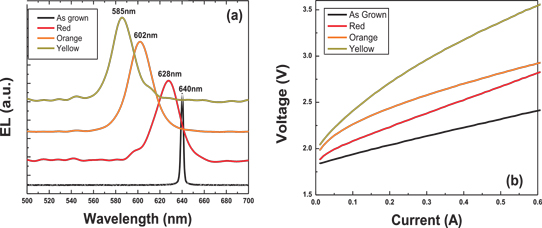
Figure 2: (a) Electroluminescence spectra for as-grown and intermixed devices emitting at 628nm, 602nm and 585nm and (b) voltage versus current characteristics of corresponding devices.
The yellow-emitting device had a turn on voltage of 2.1V, which is consistent with the bandgap of a device operating at 585nm. The series resistance of less than 5Ω is described as 'low'. "These good electrical characteristics for the yellow emitter with the highest degree of intermixing are evidence of the superiority of our intermixing process," the team writes. "In addition, the result confirms that the dopant concentration in the top contact and the cladding layers remained at a similar level and did not diffuse into the active region of the laser structure, even after the successive annealing at elevated temperatures."
Experiments varying the silicon dioxide thickness up to 2μm (2000nm) showed increasing blue-shift. However, the dielectric cracked at 2μm thickness, damaging the top surface of the semiconductor material.
Quantum well intermixing InGaP MOCVD
http://dx.doi.org/10.1063/1.4945104
The author Mike Cooke is a freelance technology journalist who has worked in the semiconductor and advanced technology sectors since 1997.


