


- News
6 May 2016
Gallium nitride light-emitting diodes, photodiodes and waveguides
Nanjing University of Posts and Telecommunications in China has been developing gallium nitride (GaN) on silicon technology with a view to monolithically integrated optoelectronic devices consisting of light-emitting diodes, photodiodes and waveguides [Wei Cai et al, Appl. Phys. Express, vol9, p052204 , 2016]. Target applications include smart transmitters/receivers for wireless visible light communication (VLC). Waveguides in GaN have high optical confinement due to the large difference in refractive index (~2.3) from that of air (~1).
The researchers comment on the particular fabricated structure (Figure 1): "The integrated device is similar to a bipolar junction transistor. The common n-contact is the base and the emitter is the LED, whereas the photodiode is the collector. The suspended waveguide is used for device connection. When the LED is turned on, photons are transported through the waveguide and absorbed in the photodiode, achieving the photonic integration of the emitter, waveguide and photodiode on a single chip."
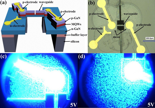
Figure 1. (a) Schematic cross section of integrated devices; (b) optical micrograph of suspended devices; (c, d) optical micrographs of light emission images obtained from silicon substrates.
The devices were fabricated from heterostructure material deposited on 2-inch GaN-on-silicon substrates. The layer structure consisted of a 900nm aluminium gallium nitride (AlGaN) buffer, 400nm of undoped GaN, a 3.2μm n-GaN contact, a 250nm indium gallium nitride (InGaN) multiple quantum well with GaN barriers, and a 220nm p-GaN contact.
Fabrication began with isolation mesa etching. Contact with the n- and p-contact regions was made with annealed nickel/gold. Waveguide structures were formed by a reactive ion etch. Silicon was also removed to give suspended membrane structuring. The wafers were then thinned on the silicon side to release the membranes. The suspended waveguide region was 60μm long, 3μm thick and 10μm wide. Removal of silicon avoids light absorption by the substrate material.
Both ends of the waveguide could emit light under current injection, although the side closer to the common n-electrode was naturally brighter. Light guided in-plane could emerge at mesa facets. Some light escaped to air from the roughened bottom surface cause by reactive ion etch. The peak electroluminescence emission was around 458.5nm wavelength at 6V bias.
The devices could be used with one for light emission and the other for photodetection. When a 10μm gap was made in the waveguide the photocurrent was much reduced, suggesting that the current was mainly induced by the guided light.
The researchers also tested the ability of both sides of the device to emit light modulated separately at 9MHz and 25MHz into free space (Figure 2). The researchers report: "The sine waves at 9MHz and 25MHz are clearly observed, indicating that the integrated devices can be feasibly used as multiple transmitters for wireless VLC applications."
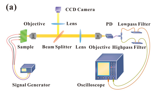
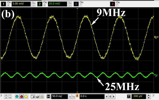
Figure 2: (a) Micro-transmittance setup. (b) Received output signals for integrated devices.
In the other direction, both devices were also tested as simultaneous photodiodes. A fiber-coupled 450nm light beam was focused on the back-side of the device with a signal that was on for 0.2 seconds and off for 0.2 seconds. A photocurrent of -42nA was induced at 0V bias. The researchers comment: "The photocurrent temporal trace shows a distinct on/off switching performance, indicating its potential use as multiple receivers for wireless VLC applications."
The same group of researchers published in March a similar device with somewhat more elaborate structure (3 p-electrodes, 3 n-electrodes, 2 sets of connecting waveguides) and more detail [Wei Cai et al, Optics Express, vol24, p6004, 2016]. In this work, the low cost of GaN on silicon is stressed. "The obvious advantages - such as use of the cheaper, widely available silicon wafer and the ability to use automated back-end manufacturing tools in silicon fabs - make mass production of monolithic photonic integration possible," the team writes.
Further, it is found that removal of the silicon substrate material from under the devices increases carrier concentrations and thus reduces resistance to current spreading. Electronic performance is also enhanced by releasing residual stress arising from lattice mismatching between the silicon substrate and III-nitride layers.
GaN LEDs Photodiodes Waveguides GaN-on-silicon
http://dx.doi.org/10.7567/APEX.9.052204
http://dx.doi.org/10.1364/OE.24.006004
The author Mike Cooke is a freelance technology journalist who has worked in the semiconductor and advanced technology sectors since 1997.


