


- News
24 May 2016
Coplanar fabricated indium gallium nitride light-emitting diodes
Xiamen University in China has created a simplified fabrication process for indium gallium nitride (InGaN) light-emitting diodes (LEDs) with a view to lower-cost display applications [H Long et al, Semicond. Sci. Technol., vol31, p065019, 2016].
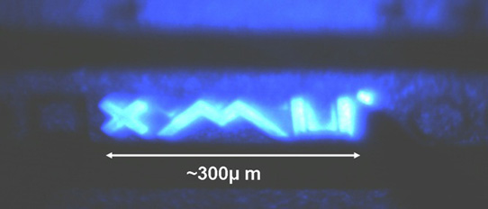
Photo: Micro-display of 'XMU' logo via coplanar LED technique.
Rather than the conventional process with mesa etching and metal contacts on two different levels, the Xiamen method produces LEDs with coplanar metal-semiconductor-metal (CMSM) contact structures on one level with one round of photolithography and electrode deposition. By contrast, the conventional process requires "at least three levels of photolithography, two steps of metal deposition and excessive chemical and thermal treatments," according to the Xiamen team.
The complicated conventional process rules out the use of LEDs as display elements on production-cost grounds, although they are now widely used as back-lighting in liquid-crystal displays (LCDs).
The metal-organic chemical vapor deposition (MOCVD) epitaxial material used for the LEDs consisted of (0001) sapphire substrate, a low-temperature GaN buffer, unintentionally doped GaN, 2μm n-GaN, a 5-period In0.15Ga0.85N/GaN multiple quantum well (MQW), 100nm of p-GaN, and 5nm of heavily doped n++-In0.15Ga0.85N. The aim of the n++-InGaN was to improve contact with the p-GaN and underlying n-GaN layers.
The contacts with the LED consisted of two concentric nickel/gold rings with inner diameters/widths of 90μm/10μm and 225μm/50μm. The fabrication consisted of electrode deposition through one step each of photolithography, magnetron sputtering, and thermal annealing at 500°C in oxygen.
Conventional mesa-type devices were also produced, with and without indium tin oxide (ITO) transparent conducting current-spreading layer (Figure 1).
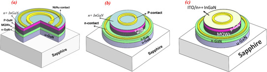
Figure 1: Schematic structure of CMSM LED (a) and conventional LEDs without (b) and with (c) ITO capping layer.
The researchers applied positive bias to the inner ring and negative bias to the outer, giving blue light emission from inside the inner ring. The emission spectrum at 20mA was around 450nm wavelength without 365nm GaN near-band-edge emission or 500nm yellow emission. This indicates that the emissions come from the MQW and not from GaN (365nm) or defect (~500nm) transitions.
The current-voltage behavior was considered to be a combination of a linear resistance of 2.3kΩ between the rings through the very thin 5nm n++-In0.15Ga0.85N layer and 100nm p-GaN and a non-linear portion from a path down from the inner ring to the n-GaN layer (p1/n), across the n-GaN layer, and then up to the outer ring. The down part of the latter current path was a forward biased p-GaN/MQW/n-GaN LED. At 20mA, the drop across this section was estimated at 3.1V, although the total was around 7.5V. The difference between 7.5V and 3.1V represents lost power (4.4Vx20mA = 88mW) and of course the quantum efficiency of the 3.1V drop will be nowhere near 100%.
The researchers comment: "Since the luminescence region was confined within the inner circle of 100μm diameter, the current density of the forward p1/n junction could be derived as 67Acm−2 at 3.1V and 20Acm−2 at 2.7V, which was similar to the electrical parameters of conventional LEDs."
The linear 2.3kΩ was estimated to be mainly through the thicker p-GaN layer rather than the 5nm n++-InGaN. The outer ring upward current path of n-GaN/MQW/p-GaN/n++-InGaN was seen as being like an npn bipolar transistor with the p-GaN/n++-InGaN junction forward biased. "Electrons from the n++ layer can diffuse into the n-layer after passing through the p-region," the researchers write.
Up to 20mA, the emission intensity was 6.7% and 11% short of the conventional LEDs without (A) and with (B) ITO current spreading, respectively (Figure 2). The performance of the CMSM LED fell further behind with greater than 20mA current injection.
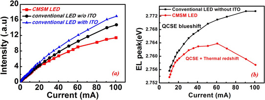
Figure 2: (a) Electroluminescence intensities of CMSM and conventional LEDs and (b) electroluminescence peak positions of CMSM LED and conventional LED without ITO as function of injected current.
The researchers estimate that at 20mA, some 3.3mA is shunted through the 2.3kΩ surface layer. At higher current, the extra self-heating of the surface region degraded the CMSM LED performance, compared with the conventional devices. Also the extra self-heating somewhat compensated the blue-shift attributed to the quantum-confined Stark effect (QCSE) that arises from electric fields caused by charge polarization of the partially ionic bonds of the III-nitride materials.
A proof-of-concept array of LEDs was produced in the shape of Xiamen University's roman initials (XMU) to indicate the potential for active-matrix (AM) and passive-matrix (PM) displays. The researchers point out that LCD external quantum efficiencies max out at 8% and theoretical organic light-emitting displays could only reach 25%. State-of-the-art GaN LEDs have efficiencies greater than 50%.
The researchers comment: "The conventional LED has the p- and n-electrodes on different planes, leading to huge difficulty in AMLED and PMLED fabrication. Our CMSM LED introduced a coplanar electrode configuration and, in our opinion, could simplify the AMLED and PMLED process."
Based on the 100μm electrode size, the estimated resolution of such displays would be around 250 pixels per inch. Although the performance of the proof-of-concept was not comparable with LCDs or OLEDs, the researchers believe that follow-up work will enhance light intensity and luminous efficiency.
InGaN LEDs InGaN LEDs GaN MOCVD
http://dx.doi.org/10.1088/0268-1242/31/6/065019
The author Mike Cooke is a freelance technology journalist who has worked in the semiconductor and advanced technology sectors since 1997.


