


- News
21 November 2016
Normally-off gallium nitride power transistor on (110) silicon
Researchers in Korea have reported a normally-off metal-oxide-semiconductor heterostructure field-effect transistor (MOS-HFET) fabricated from aluminium gallium nitride/gallium nitride (AlGaN/GaN) material grown by ammonia (NH3) molecular beam epitaxy (MBE) on (110) oriented silicon (Si) substrate [Sang-Woo Han et al, IEEE Electron Device Letters, published online 25 October 2016].
The team from Hongik University, Hanyang University and Seoul National University comments: "Demonstration of normally-off device or breakdown voltage characteristics has not been reported yet on GaN-on-Si(110) wafers to the best of our knowledge."
The researchers believe the devices have a "high potential" for power device applications and monolithic wafer-level integration of GaN power and Si (110) complementary MOS (CMOS) electronics.
Normally, epitaxial layers for GaN power transistors are grown on (111) Si. By contrast, high-performance CMOS is fabricated on (001) Si. The (111) crystal orientation of silicon has very poor electrical performance, blocking integration of GaN power with Si CMOS. The (110) Si orientation has a good structure for AlN seed layer growth and a hole mobility that is even better than the standard (001) Si orientation that is conventionally used for CMOS.
GaN power devices benefit from high breakdown fields and high electron mobility. Normally-off transistors are preferred for reduced power consumption and fail-safety. Growth on silicon should reduce material costs. Also, most commercial power devices are presently produced using silicon technology.
CMOS electronics tends to have a tighter thermal budget, compared with GaN-based devices. Ion implants, for example, suffer from dopant diffusion when subjected to raised temperature. MBE GaN growth processes generally run at lower temperature compared with the more popular metal-organic chemical vapor deposition (MOCVD).
The epitaxial structure (Figure 1) was grown on p-type Si (110) substrate in nitrogen-rich conditions supplied by ammonia MBE. The AlN growth was carried out at 900°C and the GaN growth at 780°C.
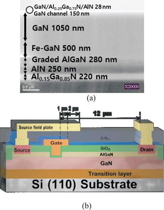
Figure 1: (a) Epitaxial structure and (b) schematic cross-section of fabricated AlGaN/GaN-on-Si(110) MOS-HFET.
The device isolation mesa was defined by inductively coupled plasma reactive-ion etch (ICP-RIE). Source and drain electrodes were titanium/aluminium/nickel/gold annealed at 820°C for 30 seconds in nitrogen. The gate region was defined by ICP-RIE down to the GaN channel. Plasma-enhanced chemical vapor deposition (PECVD) of 30nm silicon dioxide followed surface cleaning.
The 2μm-long T-gate was nickel/gold with 1μm overhangs in each direction. The source-gate and gate-drain distances were 3μm and 12μm, respectively.
The device was then annealed in oxygen at 400°C for 10 minutes to improve oxide and interface quality. Passivation was provided by 200nm of silicon nitride on which source-connected field plates were deposited.
Hall measurements gave 1640cm2/V-s electron mobility and 1.04x10¹³/cm2 carrier sheet density for the GaN channel.
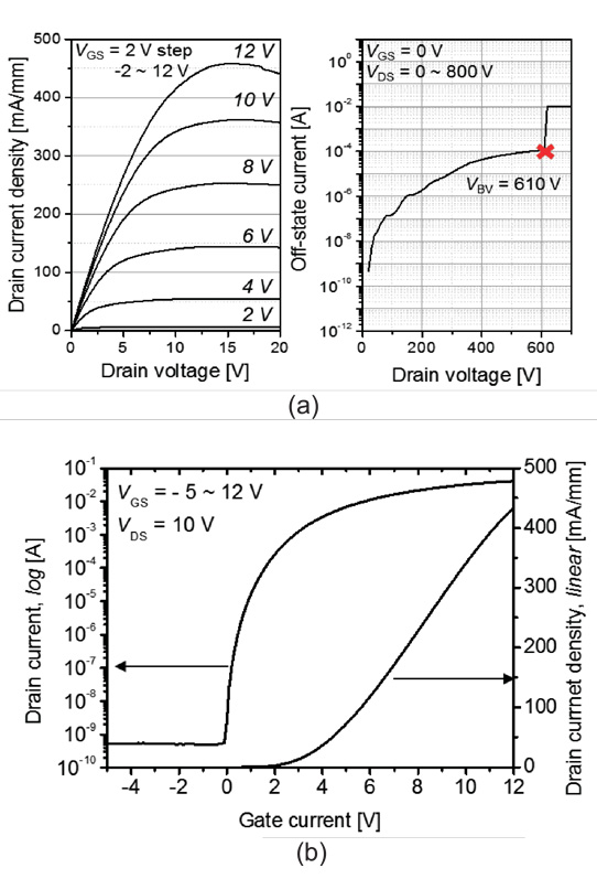
Figure 2: (a) Output and (b) transfer characteristics of fabricated AlGaN/GaN-on-Si(110) MOS-HFET.
The researchers describe their device as exhibiting "promising characteristics" with 460mA/mm maximum current density at 12V gate potential and 2.84Ω-cm2 specific on-resistance at 1V drain-bias (Figure 2). Off-state breakdown (0V gate) occurred at 610V. The on/off ratio was 108. The threshold voltage was +1.5V with a 1mA/mm threshold. Often GaN devices are normally-on (current at 0V gate potential) or only weakly normally-off (small positive threshold) with the 'off' state referring to a negative gate potential.
These performance parameters are comparable with those obtained for conventional GaN-on-(111) Si, according to the researchers.
http://dx.doi.org/10.1109/LED.2016.2621184
The author Mike Cooke is a freelance technology journalist who has worked in the semiconductor and advanced technology sectors since 1997.


