


- News
2 November 2016
Low-resistance tunnel junction boosts InGaN nanowire LED performance
McGill University in Canada has developed an indium gallium nitride (InGaN) nanowire light-emitting diode (LED) that incorporates "for the first time" a tunnel junction with a thin aluminium (Al) layer inserted between heavily doped (n++/p++) gallium nitride sections [S. M. Sadaf et al, Nano Lett. 2016, vol16, p1076, 2016]. The LED demonstrated reduced 2.9V turn-on voltage and enhanced output power compared with devices using tunnel junctions with no aluminium interlayer or without a tunnel junction.
The researchers comment: "This unique Al tunnel junction overcomes some of the critical issues related to conventional GaN-based tunnel junction designs, including stress relaxation, wide depletion region, and light absorption, and holds tremendous promise for realizing low-resistivity, high-brightness III-nitride nanowire LEDs in the visible and deep ultraviolet spectral range. Moreover, the demonstration of monolithic integration of metal and semiconductor nanowire heterojunctions provides a seamless platform for realizing a broad range of multi-functional nanoscale electronic and photonic devices."
Efficient tunnel junctions are difficult to achieve in wide-bandgap materials such as GaN. The high doping needed is particularly challenging for p-type conduction where the high activation energy of magnesium in GaN leads to low acceptor ionization efficiency. A large depletion width results across which it is difficult to tunnel.
Aluminium has a 4.08eV work function consistent with an ohmic contact with n-GaN. Defects at Al/p++-GaN interfaces "result in deep energy levels, which can significantly enhance carrier transport from p-GaN to Al in a similar manner to conventional trap-assisted tunneling," the researchers say. The quasi-ohmic characteristics of the Al/p++-GaN junction should reduce the tunneling width significantly. The Al interlayer can also reflect generated light, enhancing extraction.
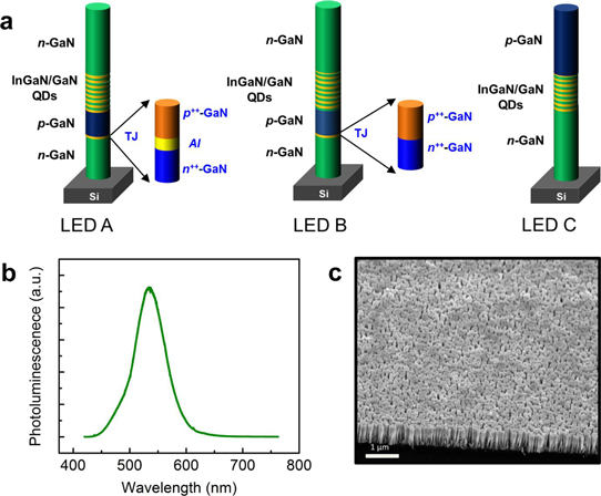
Figure 1: (a) Schematic of LEDs with Al tunnel junction dot-in-a-wire (LED A), n++-GaN/p++-GaN tunnel junction (LED B), conventional nanowire without tunnel junction (LED C). (b) Photoluminescence of LED A at room temperature. (c) Scanning electron microscope image of LED A at 45° angle.
Three types of vertical nanowire structure were produced by plasma-assisted molecular beam epitaxy (PAMBE) on n-silicon (111) substrate (Figure 1). The new structure – LED A – incorporated a tunnel junction with 7nm n++-GaN, 2nm Al, and 10nm p++-GaN. LED B used a traditional tunnel junction without the aluminium interlayer. LED C was a device without tunnel junction.
The p- and n-type regions of the devices were grown at 750°C and 780°C, respectively. The Al layer of the tunnel junction was deposited at 450°C and was capped with Ga. The p++-GaN for the tunnel junction was grown at 650°C. These temperatures were derived from series of optimization experiments. The optimized conditions achieved an Al layer that was free of voids or agglomeration.
The active regions of the devices consisted of 10 layers of strain-induced self-organized 3nm InGaN quantum dots and 3nm GaN barriers. The dots were p-doped to enhance hole injection and transport. There were no AlGaN electron-blocking layers.
Photoluminescence from the three structures was "nearly identical", according to the team, with a single peak at 534nm from the quantum dot layer. Variations in indium composition led to inhomogeneous broadening of the peak. Electron microscopy gave a density of the nanowires of the order of 1010/cm2. The diameters ranged between 40nm and 100nm.
Electron microscope and x-ray analysis suggested that the aluminium layer did not introduce performance-killing defects such as stacking faults or threading dislocations into the LED structure.
Device fabrication consisted of deposition and planarization of a polyimide resist layer, contact metalization and thermal annealing. The contacts with n-type layers were titanium/gold. The p-type contact for LED C was nickel/gold. The contacts were made to the top of the nanowires and the back-side of the silicon substrate. A 120nm indium tin oxide (ITO) transparent conducting layer was added for current spreading. The device area was 0.5mmx.0.5mm with 30% nanowire filling factor.
LED A showed a sharper turn-on of current beyond 2.9V, compared with the other devices. The specific resistance at 400mA was 4x10⁻³Ω-cm2. These values compare with a 5.5V turn-on and 5x10⁻²Ω-cm2 specific resistance for LED B with standard tunnel junction. The standard nanowire LED C without tunnel junction had an intermediate current-voltage performance.
The researchers estimate that the contribution of the Al-based tunnel junction to the series specific resistance is 1x10⁻³Ω-cm2 or lower.
Similarly, the light output under 10% duty-cycle pulsed operation from LED A was improved over that from LEDs B or C (Figure 2). The pulsed operation was designed to avoid the junction heating that occurs under continuous wave conditions. "The significantly improved light intensity is largely due to the efficient tunnel injection of holes into the active region," the team comments. The researchers also report that there was no shift in the spectrum with increasing current.
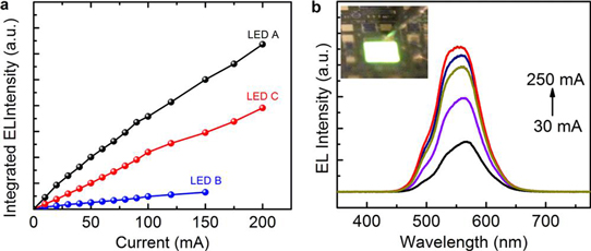
Figure 2: (a) Light output-voltage characteristics of LEDs. (b) Electroluminescence (EL) spectra of LED A under pulsed biasing. Inset optical micrograph of LED A showing strong green light emission.
The team hopes that core-shell nanowire structures could lead to high-power operation by reducing non-radiative surface recombination.
http://dx.doi.org/10.1021/acs.nanolett.5b04215
The author Mike Cooke is a freelance technology journalist who has worked in the semiconductor and advanced technology sectors since 1997.


