


- News
8 November 2016
Extending interband cascade VCSEL wavelengths to 3.4μm
The US Naval Research Laboratory and Sotera Defense Solutions in the USA have increased the wavelength of interband cascade vertical-cavity surface-emitting lasers (ICVCSELs) to 3.4μm, which "extends considerably the previous longest wavelength of 3.0μm for an electrically pumped vertical-cavity surface-emitting laser operating at room temperature," [W. W. Bewley et al, Appl. Phys. Lett., vol109, p151108, 2016].
The researchers add: "While threshold current densities as low as 390A/cm2 at 25°C are several times higher than those of the best ICL edge emitters, they are nonetheless an order of magnitude lower than for the longest-wavelength (λ ~ 3.0μm) GaSb-based ICVCSEL with type-I quantum wells demonstrated to date."
Existing mid-wave infrared (mid-IR) interband cascade lasers use long-lived interband transitions in type-II antimonide quantum wells to generate photons. Electrons are regenerated between cascade stages, as in the more complex quantum cascade lasers that use intersubband transitions.
Edge-emitting interband cascade lasers have achieved threshold currents of 100A/cm2 at an applied voltage of 4.5V in continuous-wave (cw) operation. Continuous-wave operation can be maintained up to 118°C. Wall-plug efficiencies of 18% have been reported for devices emitting in the 3μm to 6μm range.
ICVCSELs have achieved 3μm wavelengths, but with a high threshold of ~5kA/cm2 at 25°C in pulsed mode.
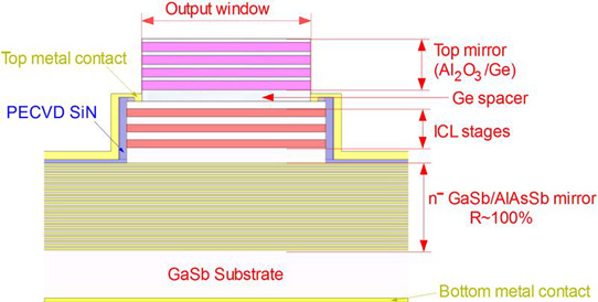
Figure 1: Schematic of ICVCSEL structure.
The ~13μm epitaxial structure for the ICVCSEL (Figure 1) was grown by molecular beam epitaxy (MBE) on n-type gallium antimonide (n-GaSb) (100) crystal orientation substrate.
The bottom mirror consisted of 22.5 pairs of n-GaSb and aluminium arsenide antimonide (n-AlAs0.08Sb0.92) quarter-wavelength layers, grown at 500°C. The n-type doping was supplied by tellurium. The doping levels in the mirror structure increased toward the layer interfaces to reduce voltage drops. Superlattices consisting of 20-period 1nm/1nm n-GaSb/n-AlAs were used for transition between the quarter-wavelength layers. The growth was monitored with a custom near-IR laser interferometer to ensure layer uniformity. The mirror was designed to have a reflectivity of 99.5%.
The mirror was separated from the active region by an n--GaSb spacer and 440°C 20nm chirped InAs/AlSb superlattice. These layers reduced the conduction band offset to a suitable level for electron injection into the active region.
The active region consisted of three groups containing five stages. The groups were separated by n--GaSb spacers. The groups were place approximately at antinodes of the resonant cavity.
The semiconductor structuring was completed with a 90nm InAs/AlSb superlattice and 100nm n+-InAs0.91Sb0.09 cap.
Fabrication consisted of dry etching circular mesas to a depth below all the active stages. plasma-enhanced chemical vapor deposition (PECVD) of 250nm silicon nitride, dry etch-back to expose the top contact window of the device, silicon dioxide sputtered and lifted-off to fill pin holes in the silicon nitride, formation of annular titanium/platinum/gold top contact on outer rim of mesa, deposition of chromium/tin/platinium/gold bottom contact on the back-side of the n-GaSb substrate, and deposition of four quarter-wavelength layers of germanium and aluminium oxide for the top mirror.
The top mirror coating extended over the mesa's sidewall. The top mirror reflectivity was estimated to be 99.3%. However, only 0.05% of the incident light was transmitted to the outside world. The researchers say that the source of parasitic absorption has not been definitively identified.
Operation consisted of 150ns pulses at 100Hz repetition. Estimated threshold currents varied with mesa diameter. With 60μm-diameter (D, 40μm-diameter emission aperture, d) devices the threshold was 390A/cm2. Smaller 30μm-diameter (20μm aperture) mesas increased the threshold to 920A/cm2. "The former value is only 2–3 times higher than the typical pulsed results for state-of-the-art edge-emitting ICLs at RT," the team writes. Smaller devices with mesa diameters of 20μm and 10μm did not lase at all.
A 50μm-diameter (40μm aperture) ICVCSEL operated up to 70°C. However, the maximum output power of the device was only 0.54mW.
While the 50μm-diameter device shows peaks separated by 1.5nm in wavelength, the smaller 30μm ICVCSEL gives a single-mode emission.
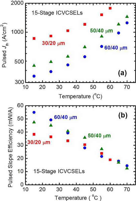
Figure 2: Threshold current densities (top) and slope efficiencies (bottom) versus operating temperature for three ICVCSELs.
The slope efficiency at 25°C ranged between 49mW/A for 60μm mesa (40μm aperture) ICVCSELs to 36mW/A for 30μm mesa (20μm aperture) ICVCSELs. The efficiency declines at increasing temperature. The researchers plan to improve the slope efficiency by refining their processing methodology. The team mainly blames high parasitic losses in the mirrors and, possibly, current spreading above threshold.
They conclude: "While the thermal impedance of the present structure is most likely too high to allow continuous-wave (cw) operation, it should be achievable with improved heat dissipation, e.g. in an epitaxial-side-down geometry. Once uniform lasing can be obtained within a smaller mesa diameter (e.g. D ~ 20μm), emission in a single spectral mode should be attainable at drive powers less than 10mW."
http://dx.doi.org/10.1063/1.4964840
The author Mike Cooke is a freelance technology journalist who has worked in the semiconductor and advanced technology sectors since 1997.


