


- News
25 November 2016
Black polycrystalline diamond transistors with high breakdown
Waseda University and Yokogawa Electric Corp in Japan have used black polycrystalline diamond (BPD) to fabricate field-effect transistors (FETs) with breakdown voltages up to 1.8kV, comparable with the performance of silicon carbide (SiC) and gallium nitride (GaN) devices [M. Syamsul et al, Appl. Phys. Lett., vol109, 203504, 2016]. Despite imperfections of the polycrystalline material such as cracks and grain boundaries, the resulting devices also achieved high maximum drain currents.
The researchers comment: "We showed that BPD-FETs may be worthy candidates for high-power FET devices, and demonstrated comparable electrical characteristics to single-crystalline diamond and clear polycrystalline diamond FETs."
Most research on diamond-based devices is based on white polycrystalline or single-crystal material. Polycrystalline silicon is widely used for thin-film transistors in displays.
Undaunted by the "unappealing large grain boundaries and cracks" of BPD, the researchers believe the material is worth further research into its full potential. "Breakdown and stress voltages of BPD in an FET have not been previously studied," they add.
The devices (Figure 1b) were fabricated on 10mmx10mmx0.5mm commercial BPD substrates produced by chemical vapor deposition (CVD). According to atomic force microscopy (AFM), the roughness was 2.72nm and grains covered 98% of the surface.
Source-drain contacts consisted of gold/titanium layers. The electrodes were annealed at 450°C for 30 minutes in hydrogen. This formed a layer of titanium carbide (TiC) between the titanium contact and carbon material of the BPD. After annealing, the sample was heat treated with hydrogen plasma at 600°C for 6 minutes.
A narrow 25μm-wide horizontal two-dimensional hole gas (2DHG) channel was defined with photoresist. The 2DHG was created using treatment involving ultraviolet light and ozone, giving a partially carbon-oxygen (C-O) bond surface termination. This gave a potential barrier of 2eV between the carbon-hydrogen bonded 2DHG region and the surrounding C-O terminated areas, giving electrical isolation of the channel.
The photoresist was removed and a 200nm aluminium oxide (Al2O3) gate dielectric layer built up using alternate exposures to trimethyl-aluminium and water (H2O) at 450°C.
The device was completed with the removal of Al2O3 from the source-drain areas and deposition of the aluminium gate electrode.
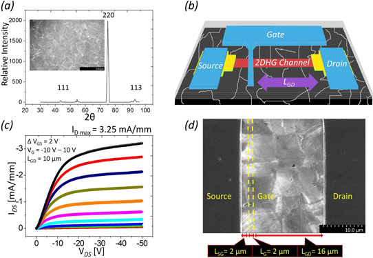
Figure 1: (a) X-ray diffraction pattern of BPD. Inset: field-emission scanning electron microscope image of rough BPD surface. (b) Diagram of BPD-FET. (c) Drain current–voltage (IDS–VDS) characteristics in vacuum at room temperature with LGD of 10μm. (d) Field-emission scanning electron microscope image of region between the source and drain of the BPD-FET after stripping metallization and Al2O3 passivation.
Measurements (Figure 1c) were made on a device with 10μm gate-drain distance (LGD), 2μm gate length (LG) and 2μm source-gate distance (LSG) in vacuum. "The characteristics of the saturation curves, including the pinch-off and saturation region, were similar to those of single-crystalline or clear-type polycrystalline diamond FETs, exhibiting nearly perfect modulation," the team comments.
The maximum drain current (IDmax) was 3.25mA/mm. The researchers point out: "The maximum drain current was unusually high for BPD considering the room-temperature operation and 25μm channel width. This value is also nearly three times higher than the boron-doped metal-semiconductor field-effect transistors (MESFETs) and junction field-effect transistors (JFETs)."
Increasing LGD to 18μm enabled a breakdown voltage (VB) of 1824V with IDmax of 1.1mA/mm. The team claims: "These findings indicate that our BPD-FET has the highest breakdown voltage of any diamond FET reported to date. The breakdown voltage was more than 300V higher than boron-doped diamond FETs and three times greater than JFETs."
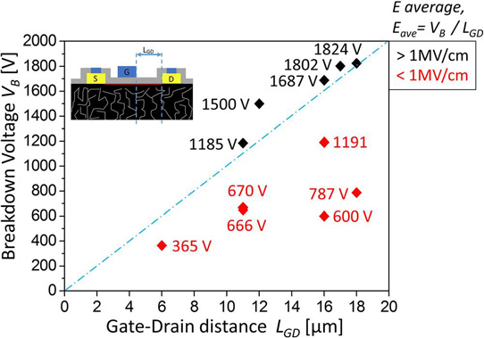
Figure 2: Breakdown voltage versus LGD – those above the dashed line satisfy VB/LGD greater than 1MV/cm.
Over a range of devices with varying LGD values, the average electric field at breakdown (VB/LGD) reached as high as 1.25MV/cm. Values greater than 1MV/cm are taken as indicative of high-voltage robustness in FETs, according to the researchers. Out of ten devices presented in the paper, five met this criterion (Figure 2).
Aluminium gallium nitride barrier/gallium nitride (AlGaN/GaN) channel FETs have achieved values of VB/LGD up 1.7MV/cm. The researchers comment that their devices have demonstrated among the highest values for planar FETs, adding: "Performance of our BPD-FETs exceeded those of Ga2O3, SiC and AlGaN/GaN based devices, which have shown VB/LGD values of 0.5, 0.8, and 1MV/cm, respectively."
The researchers also studied the degradation of the devices after subjecting them to harsh voltage stresses. The degradation in IDmax after 500V stress was 6% for a 16μm LGD from 2.42mA/mm, before, to 2.28mA/mm, after. A 1000V stress reduced I-{Dmax} further to 1.81mA/mm (25% down on the original value). Breakdown occurred at 1191V. Voltage stress of 2000V destroyed the device.
The team believes that better understanding of the effect of polycrystalline grain boundaries on high voltage breakdown could lead to further improvements in BPD-FET devices.
Black polycrystalline diamond FETs CVD
http://dx.doi.org/10.1063/1.4967999
The author Mike Cooke is a freelance technology journalist who has worked in the semiconductor and advanced technology sectors since 1997.


