


- News
26 October 2016
Silicon germanium light-emitting diodes on silicon on insulator
Xiamen and Nankai universities in China have jointly developed lateral p-i-n silicon germanium/germanium/silicon germanium (SiGe/Ge/SiGe) light-emitting diodes (LEDs) with high luminous extraction compared with a vertical design [Guangyang Lin et al, Appl. Phys. Lett., vol109, p141104, 2016].
An efficient Ge-based light-emitting device is highly desired as part of the drive to Si-based optoelectronic integrated circuits. Since germanium has a narrower bandgap than silicon, generated light could be used in silicon photonic structures that require wavelengths longer than 1.1μm.
The impediment to using Ge in this way is its indirect bandgap, which makes for very inefficient electron-hole recombination into photons. However, the difference between the indirect minimum and direct transitions between the conduction and valence bands is only about 136meV, giving a 'quasi-direct' gap. This difference can be further reduced by applying tensile strain.
On the processing side, Ge is already used in many mainstream silicon electronics enhancements such as 'strained silicon' transistors and in SiGe bipolar transistors. This is in contrast to standard direct-bandgap light-emitting III-V compound semiconductors made of materials that poison the performance of standard silicon components.
Some vertical LEDs using various SiGe combinations have been developed. The Xiamen/Nankai researchers believe that lateral junctions could be a better choice in terms of reducing carrier loss in defect-rich Ge buffer layers at the Ge/Si interface, light absorption in metal contacts, and self-absorption in Ge. "So far, few works were reported on Ge lateral junction light-emission diodes, especially with lateral heterojunctions," they write.
The Xiamen/Nankai epitaxial structure was grown on a germanium 'virtual substrate' (VS) on silicon on insulator (SOI). Six 9nm Ge quantum wells were separated by 15nm Si0.13Ge0.87 barriers. The structure was annealed at 800°C for 60 seconds, intermixing the 6x(SiGe/Ge) structure to give a uniform SiGe layer. Raman analysis suggests that the resulting 159nm layer consisted of 95% Ge with ~1% strain. The strain in the underlying Ge was ~0.3%.
The researchers comment that the high annealing temperature of 800°C enhanced the tensile strain due to the difference in thermal expansion coefficients between silicon and germanium. "The tensile-strained SiGe overlayer can also act as an external strain source leading to larger tensile strain in the Ge VS, which is beneficial for achievement of direct band luminescence from Ge," they add.
Fabrication (Figure 1) included dry etching down to the buried oxide insulator layer to give 10μm-wide waveguides, dry etching the SiGe layer to form a lateral double heterojunction (SiGe/Ge/SiGe), ion implantation to form p- and n-type SiGe contacts, doping activation at 650°C for 15 seconds, encapsulation in silicon dioxide, formation of contact holes and deposition and patterning of aluminium electrodes and wiring. The team says that the fabrication process is CMOS-compatible, paving the way for integration with Ge MOSFETs.
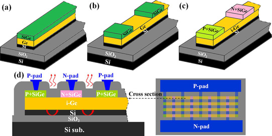
Figure 1: Fabrication flow of lateral p-SiGe/i-Ge/n-SiGe heterojunctions on SOI substrates: (a) SiGe/Ge/Si waveguides on SOI, (b) SiGe/Ge/SiGe lateral heterojunctions on waveguides, (c) selective ion implantation to form P+ and N+ SiGe regions, and (d) schematic of top view and cross sections.
Vertical p-i-n Ge homojunction devices were also fabricated on SOI with a similar area for comparison.
As the current injection in the lateral device was increased electroluminescence (EL) around 1600nm (1.6μm) wavelength was detected by an indium gallium arsenide (InGaAs) on indium phosphide (InP) photodetector (Figure 2). Red-shift was seen at higher currents due to Joule heating. At 2.5kA/cm2 current injection, the peak intensity for the lateral heterostructure device was 4x that of the vertical homojunction structure. "In addition, the EL peak position of the lateral heterojunction locates at the higher-energy side compared to the vertical homojunction, which might be attributed to modification of spectra by the cavity effect and/or weaker Joule heating effect," the researchers write.
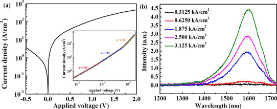
Figure 2: (a) Typical current density-voltage characteristic of heterojunction diode. Inset: forward bias curve in log-log scale marked with extracted ideality factors; (b) electroluminescence spectra under various injection current densities.
The increase in intensity with current for 20μm- and 2μm-wide i-Ge region lateral devices is approximately quadratic (1.9 current-exponent for 20μm, 2.0 for 2μm), consistent with theoretical considerations of large carrier injection. The 20μm peak intensity is about 3x that of the 2μm device.
Light extraction from the device also benefits from reflection off the silicon dioxide/silicon interface of the SOI substrate, giving enhancement from a cavity resonance effect.
http://dx.doi.org/10.1063/1.4964385
The author Mike Cooke is a freelance technology journalist who has worked in the semiconductor and advanced technology sectors since 1997.


