- News
4 October 2016
Oxford Instruments develops SiC via etch for GaN-on-SiC RF device manufacture
UK-based process equipment maker Oxford Instruments has announced the development and launch of a silicon carbide (SiC) via plasma etch process using its PlasmaPro100 Polaris etch system.
SiC is becoming an increasingly important material, particularly for gallium nitride (GaN) RF devices using SiC as a substrate. A smooth via etch through the SiC is essential to enable these devices. Oxford Instruments says that it has developed a solution for etching high-quality SiC vias efficiently. Combined with a low-damage GaN etch within the same hardware, the PlasmaPro100 Polaris offers what is claimed to be a unique capability for GaN-based RF device plasma etch processing requirements.
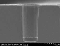
 Picture: SEM showing smooth via etch through SiC.
The new technology offers several process capabilities suited to the SiC via application:
- high SiC etch rate, enabling maximum throughput;
- smooth sidewalls for problem-free post-etch metallization;
- high selectivity to underlying GaN layers, giving a smooth, low-damage stop onto the GaN device layers;
- clamping of sapphire carriers using Oxford Instruments' patented Electrostatic Clamp technology, ensuring sample temperature control and maximum yield;
- capability of etching SiC and GaN in the same tool through advanced plasma source technology; and
- high utilization provided by long mean time between cleans (MTBC).
"Our applications specialists have spent significant time developing this SiC via etch process on the PlasmaPro100 Polaris etch system, enabling high selectivity and throughput, amongst other benefits," says Dr Mark Dineen, optoelectronics product manager at Oxford Instruments Plasma Technology (OIPT). "These benefits will enable our customers to etch both SiC and GaN in the same tool through advanced plasma source technology."
www.oxford-instruments.com/plasma


