


- News
12 October 2016
Integrating gallium nitride LED with silicon drive transistor
Toyohashi University of Technology in Japan has developed a wafer bonding technique to combine silicon metal-oxide-semiconductor field-effect transistor (MOSFET) electronics with gallium nitride (GaN) micro-light-emitting diodes (μLEDs) [Kazuaki Tsuchiyama et al, Appl. Phys. Express, vol9, p104101, 2016]. The researchers also see prospects for integrating silicon electronics with high-voltage/high-frequency GaN transistors.
The electronics were fabricated in a 340nm silicon layer on 400nm buried silicon dioxide (SiO2, BOX) electrical insulator on a GaN LED wafer (Figure 1). The researchers comment: "With such a structure, the thermal decomposition of the GaN layer and the contamination of the Si layer under a high-temperature process can be prevented because the GaN layer is capped with the top-Si layer during the Si device process."
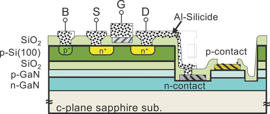
Figure 1: Schematic cross section of GaN-μLED driver circuit consisting of Si n-MOSFET and GaN-μLED.
The layer thicknesses were also chosen to avoid cracking, since thicker layers tend to crack due to mismatches in thermal expansion coefficients.
The transistor structure was fabricated before selective etch that removed silicon materials from the region where LEDs were planned. Finally, metal wiring, including the gate electrode, was deposited to form the n-MOSFET drive circuit and μLED combination.
The team comments: "This structure and process flow had high compatibility with a traditional Si planar process, and thus the utilization of a Si CMOS process line was possible."
The Si/SiO2/GaN structure was created using surface-activated bonding of silicon-on-insulator (SOI) and GaN-LED on sapphire wafers. The buried oxide came from low-pressure chemical vapor deposition of silicon dioxide on the GaN-LED wafer. The silicon handle of the SOI wafer was removed by grinding and dry etch. The doping of the MOSFET regions was achieved by ion implant with a plasma-enhanced chemical vapor deposition (PECVD) layer of SiO2. The n-type source and drain regions (S/D) were achieved with phosphorus doping and the p+ body contact (B) with boron. The gate insulator was SiO2 from a high-temperature (900°C) wet oxidation. The high temperature also annealed and activated the doping implants.
The LEDs consisted of mesa structures with annealed titanium/aluminium/titanium/gold n- and nickel/silver/nickel p-contacts.
The MOSFET gate electrode was aluminium rather than the more usual polysilicon. The wafer was passivated with more PECVD SiO2 in which contact holes are etched out. Aluminium silicide (Al-Si) was sputtered and patterned to give the wire connections between components.
The size of the LED was 30μmx30μm. The n-MOSFET gate was 10μm long and 100μm wide. The researchers give the LED/MOSFET footprint ratio as approximately 0.125.
Characterization of independent n-MOSFETs on the same wafer gave a threshold voltage of about 0.8V at 5V drain bias. The transconductance was 0.62mS/mm. Independent LEDs achieved an external quantum efficiency (EQE) of 6.7% and a turn-on voltage of 3V. The spectral peak was around 460nm wavelength with 22nm full-width at half-maximum (FWHM). The LED performance was similar to that of devices fabricated on raw GaN LED substrates without silicon layers.
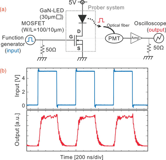
Figure 2: (a) Pulse driving system for evaluating dynamic characteristics of GaN-μLED driver circuit. (b) 1MHz input voltage signal applied to gate of Si n-MOSFET (blue) and light output response emitted from GaN-μLED (red).
The MOSFET-LED integrated circuit was tested for up to 10MHz pulse modulation with a square signal delivered to the gate of the MOSFET (Figure 2). The response of the circuit showed the effects of parasitic capacitance that will need to be reduced for higher-bandwidth performance.
The researchers point out that the 5μm design rule used in the CMOS fabrication is equivalent to what was used in 1970s ~10MHz microprocessors. The team suggests that scaling down the design rule would increase performance without LED drivability deterioration.
Wafer bonding SOI GaN-on-sapphire LEDs MOSFETs
http://doi.org/10.7567/APEX.9.104101
The author Mike Cooke is a freelance technology journalist who has worked in the semiconductor and advanced technology sectors since 1997.


