


- News
26 September 2016
Reducing subthreshold swing of gallium arsenide transistors
Korea Institute of Science and Technology (KIST) claims a record low subthreshold swing of 68mV/decade for a gallium arsenide (GaAs) field-effect transistor (FET) [SangHyeon Kim et al, IEEE Electron Device Letters, published online 24 August 2016]. In addition, the double-gate (DG) device on insulator (OI) was fabricated on silicon through wafer bonding.
The team comments: "Combining other device technologies, DG GaAs-OI FETs will be a promising component technology in future III-V transistors on the Si platform."
GaAs is a III-V semiconductor with higher mobility than silicon, and it is hoped that incorporating III-V materials on silicon could be a way forward to faster and/or lower-power-consuming electronics.
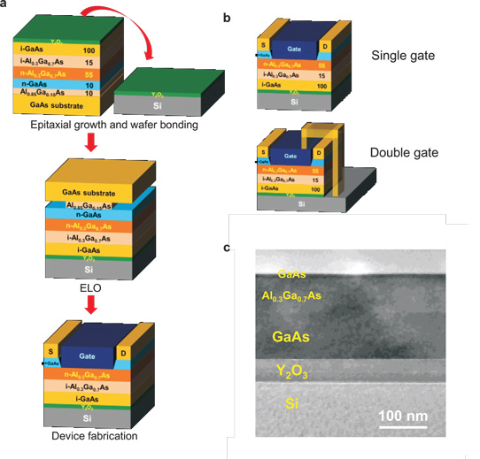
Figure 1: (a) Fabrication process flow of GaAs-OI FETs on Si via wafer bonding and ELO. Thicknesses of each layer are also shown (nm). (b) Schematic images of final device structures of SG and DG GaAs-OI FETs. (c) Cross-section transmission electron micrograph of fabricated GaAs-OI FETs on Si substrates.
The KIST transistor structure (Figure 1) was grown on GaAs (100) substrates using molecular beam epitaxy (MBE). The III-V material was bonded to silicon using oxygen-plasma-activated yttrium oxide (Y2O3) layers deposited on the heterostructure and silicon substrate through electron-beam evaporation. The bonding was carried out at room temperature with 180kg force.
The Y2O3 forms a buried oxide layer in the final device with a relatively high dielectric constant (k) of 16. The high Young's modulus of 215GPa gives a strong bond between the materials. Trivalent oxides like Y2O3 also give good metal-oxide-semiconductor (MOS) interfaces with III-V semiconductors.
The transistor heterostructure was separated from the GaAs growth substrate by epitaxial lift-off (ELO) wet etch of an aluminium gallium arsenide (AlGaAs) sacrificial layer.
Single-gate (SG) and double-gate transistors were produced. The top gate consisted of recessed platinum/gold on an AlGaAs barrier/insulator layer. The source/drain electrodes were platinum/germanium/gold. The metals were annealed. Double-gate devices were formed by making a connection between the top gate and the silicon substrate acting as a back gate with Y2O3 insulator giving a MOS structure.
The researchers claim a record low subthreshold swing for GaAs FETs of 68mV/decade for the double-gate transistor. This beats a 2015 report of 70mV/decade for a GaAs-AlGaAs core–shell nanowire transistor. The SG swing was around 85mV/decade. The theoretical minimum is ~60mV/decade at room temperature. The on/off current ratio was also very high at around 108.
"These good electrical properties were attributed to the DG device structure via the tight control of channel carriers," the team writes.
Thanks to a low subthreshold current, the threshold voltage of the DG transistor was higher than that of the SG device. The transconductance was also boosted by about 37% in the DG structure at 0.5V and 0.05V drain biases.
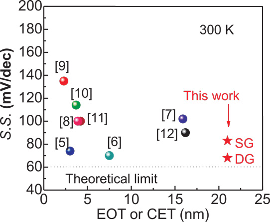
Figure 2: Subthreshold swing benchmarks for state-of-the-art GaAs FETs as function of EOT or CET.
The equivalent oxide thickness/capacitance equivalent thickness (EOT/CET) was somewhat larger than previously reported devices (Figure 2). The KIST device was the only one on silicon – the other reported transistors were fabricated on GaAs substrates.
The researchers comment that device fabrication has not been optimized and there is a wide opportunity to scale down EOT. One optimization option could be to balance the top and bottom controllability of the gates.
GaAs FET GaN FET GaAs AlGaAs MBE
http://ieeexplore.ieee.org/document/7549103/
The author Mike Cooke is a freelance technology journalist who has worked in the semiconductor and advanced technology sectors since 1997.


