


- News
21 September 2016
Reducing laser diode optical leakage with indium gallium nitride waveguides
Institute of High Pressure Physics (IHPP) and TopGaN Ltd, both of Poland, have been jointly developing indium gallium nitride (InGaN) waveguide structures for use in blue laser diodes (LDs) [Grzegorz Muziol et al, Appl. Phys. Express, vol9, p092103, 2016)]. The aim is to improve beam quality for applications such as data storage and image projectors.
Beam quality in III-nitride semiconductor laser diodes suffers because of optical leakage to the substrate through the bottom aluminium gallium nitride (AlGaN) cladding. Thicker cladding layers reduce leakage, but the thickness of AlGaN layers is restricted for coherent straining to GaN and for avoiding the cracking of epitaxial layers.
The IHPP/TopGaN team proposes the use of InGaN waveguides with thickness and indium content sufficient to increase the effective refractive index to greater than that of GaN. This should not only reduce leakage, but fully suppress it, according to the researchers. They comment: "The most important advantage of this design is that a thick n-AlGaN cladding is not necessary to obtain high optical beam quality."
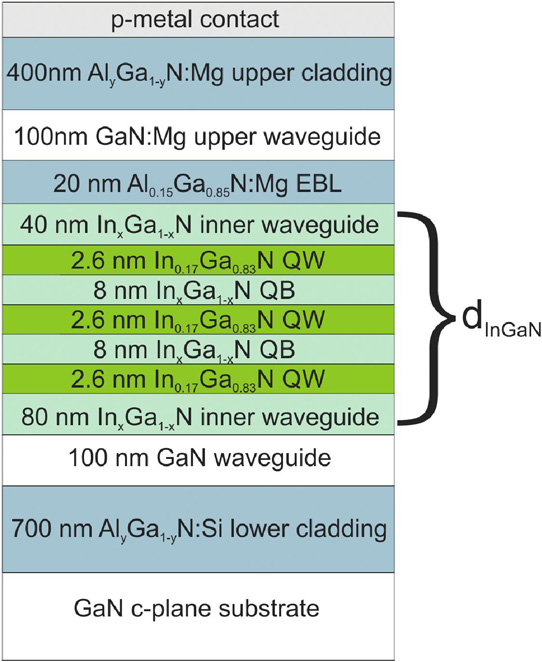
Figure 1: Schematic design of laser diode.
The researchers used plasma-assisted molecular beam epitaxy (PAMBE) to grow the material for blue laser diodes with InGaN waveguides (Figure 1). Eight different InGaN waveguide structures were grown, aiming to validate simulations previously developed by the team. The AlGaN cladding had fixed thicknesses of 700nm and 400nm and Al composition of 6% Al. The 700nm lower cladding thickness would allow significant optical leakage into the substrate without waveguide layers.
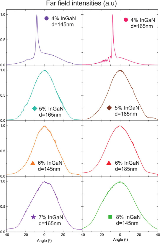
Figure 2: Experimentally measured fast axis of laser diode far-field patterns with various InGaN waveguide compositions and thicknesses.
The far-field profiles were assessed using a CCD camera (Figure 2). The diodes with the lowest-indium-content waveguides showed the effects of leakage into the substrate in the form of an "enormous narrow peak" at 9.5° with 145nm In0.04Ga0.96N waveguide layers. The intensity maximum was 7x that of the main Gaussian profile.
The researchers comment: "This is a manifestation of a strong leakage to the GaN substrate. It is so strongly pronounced because the thickness of the n-AlGaN cladding layer is insufficient to reduce it. If the thickness would be higher, the leakage and thus the magnitude of the peak could be reduced. The amount of light in this peak is 25% of the overall far-field pattern and agrees well with the value of 21% predicted theoretically."
The width and height of the measured peak is broader and shorter than the simulations, however. The team suggests that this could be due to small inhomogeneities of electron concentration, affecting the refractive index.
The InGaN waveguides with indium content higher than 5% had no visible leakage peaks, in line with the modeling.
Institute of High Pressure Physics TopGaN InGaN InGaN waveguide Blue laser diodes PAMBE
http://doi.org/10.7567/APEX.9.092103
The author Mike Cooke is a freelance technology journalist who has worked in the semiconductor and advanced technology sectors since 1997.


