


- News
26 September 2016
Two-dimensional gallium nitride with graphene encapsulation
Researchers in the USA have grown two-dimensional (2D) layers of gallium nitride (GaN) using a graphene encapsulation on silicon carbide (SiC) substrate [Zakaria Y. Al Balushi et al, Nature Materials, published online 29 August 2016]. The team from Pennsylvania State University, University of Notre Dame, US Naval Research Laboratory, University of Texas at Dallas, and Physical Electronics USA comments: "Graphene has proven to be a remarkable material over the past decade; and with the discovery that it can stabilize 2D forms of traditionally '3D' binary compounds, we have provided the foundation to realize many other classes of materials that are not traditionally 2D."
Such 2D GaN is expected to have a different vibrational/phonon structure with respect to bulk material that could modify polaritonic photon–phonon mixing behavior with possible nanophotonic application in the mid-infrared.
The researchers hope that the process could lead to new heterostructures of 2D layered materials, including those from the III-nitride group to which GaN belongs.
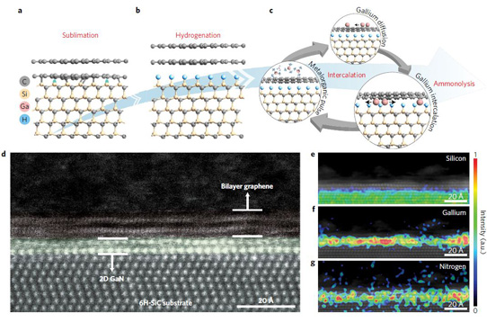
Figure 1: a–c, Schematic of MEEG process for 2D GaN (d). Green halos at SiC/graphene interface represents silicon dandling bonds. d, High-angle annular dark-field scanning transmission electron microscope cross-section of 2D GaN. e–g, Elemental energy dispersive x-ray mapping of silicon (e), gallium (f) and nitrogen (g) in 2D GaN.
The researchers first sublimated silicon from the surface of the SiC (0001) substrate at ~1600°C in argon to give a layer of quasi freestanding epitaxial graphene (QFEG, Figure 1). The graphene layer was hydrogenated to passivate dangling bonds. The graphene on SiC structure was exposed to cycles of trimethyl-gallium at 550°C with Ga adatoms inserting themselves between the graphene and SiC. The intercalated Ga was transformed at 675°C into 2D GaN with the nitrogen supplied by ammonia decomposition.
It was found that the (MEEG) process resulted in two layers of GaN encapsulated by a bilayer of graphene. Examination of the sample showed that the intercalation was facilitated by defects of the graphene structure (point-, wrinkles, metal-graphene interactions). The MEEG process also causes increased defects in the graphene over regions of 2D GaN.
The researchers also used the MEEG process to produce thicker, more-than-5nm layers of 2D GaN. The surface termination of the 2D GaN was similar to that found with the two-layer GaN.
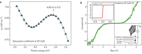
Figure 2: a, Absorption coefficient (α) of 2D GaN from ultraviolet–visible spectroscopic ellipsometry, revealing direct Eg of 4.98 eV. Connecting line is to guide eye. b, Vertical transport measurements with 2D GaN Schottky barrier. Current–voltage curve of heterostructure (green) and QFEG/6H-SiC (red curve in top-left inset) collected with conductive AFM (bottom-right schematic).
Ultraviolet-visible reflectance measurements found an inflection point at 4.90eV, not observed in samples without GaN (Figure 2). The researchers therefore believe that 4.90eV represents the region of the bandgap energy (Eg) of the 2D GaN. Density functional theory (DFT) calculations predict values of 4.79eV and 4.89eV, according to different approximations. Another approach using absorption coefficients in the ultraviolet–visible range gave a direct bandgap of 4.98+/-0.13eV. These values are much higher than the 3.42eV of normal bulk GaN.
The researchers also used low-loss electron energy-loss spectroscopy (EELS) measurements on material with the graphene encapsulation removed, resulting in a 5.53eV bandgap. The team comments: "The ~0.6eV deviation in the Eg measured from low-loss EELS arises from specular losses, such as Cerenkov loss, that are observed in EELS measurements of high-dielectric materials. Our results, however, provide direct evidence that the Eg is much larger than that found in bulk GaN, with theoretical and experimental values being in good agreement."
Vertical current flow was also measured using conductive atomic force microscopy (AFM). Forward bias flow is believed to be mainly electrons pulled from the accumulated n-type 6H-SiC over a ~1.7V conduction band offset between SiC and 2D GaN. The reverse flow is tentatively attributed to "electron injection from graphene over the Schottky barrier provided by 2D GaN, and into the depleted n-type 6H-SiC". Away from the regions of 2D GaN the conduction was ohmic (i.e. approximately linear).
Analysis suggests the 2D GaN regions were in a buckled state and the stoichiometric composition was not 1:1. The layer was covalently bonded with the underlying SiC; the bonding with the graphene encapsulation was van der Waals.
Two-dimensional GaN GaN Graphene encapsulation SiC
http://dx.doi.org/10.1038/nmat4742
The author Mike Cooke is a freelance technology journalist who has worked in the semiconductor and advanced technology sectors since 1997.


