


- News
26 April 2017
Buffer and drift layer effects on vertical gallium nitride diodes
Arizona State University in the USA has been studying the effects of gallium nitride (GaN) buffer layer thickness and drift layer doping on the performance of vertical p-n and Schottky barrier diodes [Houqiang Fu et al, IEEE Electron Device Letters, published online 4 April 2017]. Without passivation or field plates, some p-n devices reached breakdown voltages of more than 1000V and achieved specific on-resistances as low as 3mΩ-cm2.
Free-standing GaN substrates are being studied for use in vertical devices because high material quality is needed to avoid premature breakdown through defects in power electronics. Such substrates are more expensive than more conventional sapphire or silicon carbide (SiC) wafers. Defect densities of GaN on sapphire or SiC tend to be more than 109/cm2. Using free-standing substrates can reduce the density to around 106/cm2. Further effects on material quality come from varying the buffer and drift layers, the focus of Arizona’s work.
Samples were created from metal-organic chemical vapor deposition (MOCVD) on n-GaN free-standing substrates (Figure 1). The buffer layer was doped with silicon at 2x10¹⁸/cm3 concentration. The buffer thickness was varied at 50nm, 400nm, 1μm and 1μm for samples A-D, respectively. The 9μm drift layer was unintentionally doped (UID), except for sample D that was lightly doped with silicon (2x10¹⁶/cm3). The p-GaN upper layers were doped with magnesium – 500nm at 1019/cm3 concentration and 20nm at 1020/cm3.
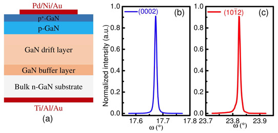
Figure 1: (a) Schematic of GaN p-n diodes on bulk GaN substrate. High-resolution x-ray diffraction rocking curve of (b) (0002) plane and (c) (10-12) plane for GaN p-n diodes.
As a result of x-ray diffraction analysis, the researchers comment: “All samples have dislocation densities on the order of 106/cm2 , which are significantly lower than that of typical GaN devices grown on sapphire (> 109/cm2 ).” Atomic force microscopy scans gave root-mean-square roughness values in the range 0.5-1.5nm over a 10μmx10μm field.
The p-n diode fabrication began with inductively coupled plasma etch to 1.5μm depth of 260μm-diameter circular mesas. Annealed 200μm-diameter p-GaN ohmic contacts of palladium/nickel/gold (Pd/Ni/Au) were created with electron-beam evaporation. The backside n-GaN contacts were titanium/aluminium/gold (Ti/Al/Au).
The p-n diode turn-on voltage for all samples was around 3.1V. The on/off current ratio was of the order 1010. Variations between devices are not believed to be intrinsic, but rather due to inhomogeneous p-contact resistance. The specific on-resistance was of order 3mΩ-cm3 at 4V.
Electroluminescence was detected with spectral peaks at 2.2eV, 3.2eV and 3.4eV photon energies. “The strong EL suggests the radiative recombination in GaN p-n diodes and is an indication of high material quality,” the researchers write.
The reverse-bias breakdown voltage was highest at more than 1000V for the p-n diode on sample C. The other samples in order of decreasing breakdown voltage were B at 772V, D at 687V, and A at 647V. The sample C device had a thicker buffer layer and low drift layer doping.
Some Schottky barrier diodes were also produced with Pd contacts on samples where the MOCVD growth ended with the drift layer. The buffer layer thicknesses were 20nm, 100nm, 400nm and 400nm for SBDs1-4, respectively. The buffer silicon doping was at 2x10¹⁸/cm3, as before. The 9μm drift layer was unintentionally doped, except for SBD4 with light silicon doping (2x10¹⁶/cm3).
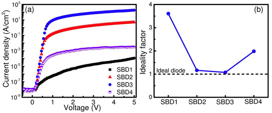
Figure 2: (a) Forward current-voltage I–V characteristics and (b) ideality factor of GaN Schottky diodes.
The SBDs showed much more variation in on-current, with SBD3 demonstrating the highest (Figure 2). Also, the ideality for SBD3 was near unity at 1.07, indicating high material quality of the drift layer, according to the team. The researchers comment: “With the same UID drift layer, the ideality factor decreases with increasing buffer layer thickness, indicating thicker buffer layer results in better material quality which can result from reduced defect density.”
Thinner buffers and intentional drift layer doping gave idealities deviating from near-unity.
Thicker buffers were also found to increase the critical electric field, and hence breakdown voltages. However, the critical electric field was smaller than previous work by University of Notre Dame and Cornell University. The Arizona team attributes the lower performance to insufficient mesa isolation and larger contacts.
The breakdown characteristics of the SBDs followed the trends of the p-n diodes with the best performance coming from thicker buffers and lower drift layer doping.
One negative side-effect of the having thicker buffers was to increase the net doping in the overlying drift layer, which potentially could impact performance, according to capacitance-voltage studies on the SBDs. However, the researchers found that drift layer material quality was more important than doping concentration in achieving high breakdown voltages.
GaN GaN buffer layer thickness Drift layer doping Schottky barrier diodes MOCVD
https://doi.org/10.1109/LED.2017.2690974
The author Mike Cooke is a freelance technology journalist who has worked in the semiconductor and advanced technology sectors since 1997.


