


- News
28 April 2017
Monolithic gallium nitride vertical transistor and light-emitting diode
South China University of Technology and Hong Kong University of Science and Technology (HKUST) claim the best performance ever reported for the monolithic integration of gallium nitride (GaN) light-emitting diodes (LEDs) with driving transistors [Xing Lu et al, IEEE Electron Device Letters, published online 6 April 2017]. The team used a combination of dry and wet etch, along with selective epitaxial regrowth, to produce vertical metal-oxide-semiconductor field-effect transistors (VMOSFETs) alongside LEDs.
Presently, LEDs are combined with dedicated and bulky electronic driving circuits to achieve functions such as AC-DC conversion, current sourcing, and dimming. The parts are connected using bonding wires that introduce parasitic elements that sap performance in terms of high power consumption and low efficiency. LED systems often fail through the peripheral parts and packaging rather than through the LED chip itself.
Apart from the problems of having separate devices for light emission and electronic control, GaN transistors offer potential benefits of large breakdown voltage, fast operation speed, low power loss, and high temperature endurance. The researchers comment: “By integrating GaN-based LEDs and driving transistors on the same substrate, a compact smart-lighting system can be realized and benefit a range of applications such as solid-state lighting, micro-displays and visible light communications (VLCs).”
The VMOSFET structure results in enhancement-mode operation, which simplifies drive circuitry by allowing use of a single-polarity voltage supply. The team sees an added advantage: “VMOSFETs share similar junction-based vertical structures with LEDs and are more suitable for integration than the lateral ones.”
To realize VMOSFETs with high performance, the etch process needs to maintain GaN crystal quality of the sidewalls of trenches through which channel currents flow. Dry etching using plasma tends to result in rough, damaged surfaces. Wet etch is often used to clean up after such processes.
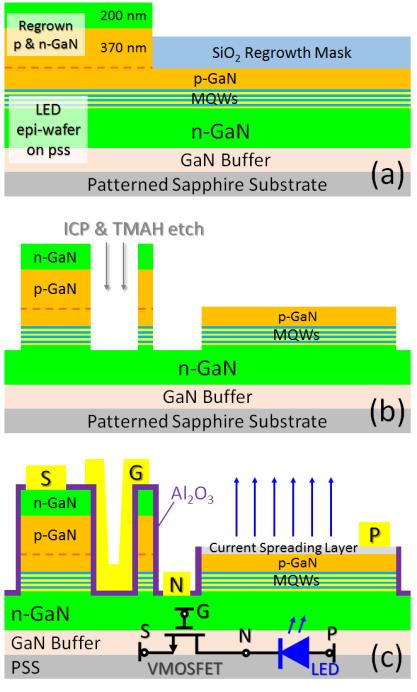
Figure 1: Main steps in fabricating monolithically integrated VMOSFET-LED device: (a) selectively re-grow p- and n-GaN bilayer on LED; (b) gate trenches and device isolation etching; (c) fully processed device.
The researchers used 2-inch GaN LED on patterned sapphire substrates (pss) with InGaN/GaN multiple quantum wells. The fabrication of the VMOSFET-LED began with plasma-enhanced chemical vapor deposition (PECVD) silicon dioxide that was patterned using a buffered oxide etch to give a re-growth mask (Figure 1). The re-grown material selectively added p- and n-GaN layers to give an n/p/n structure.
Etching for the gate trench and for electrical isolation were achieved by a combination of inductively coupled chlorine plasma dry and tetramethylammonium hydride (TMAH) wet processes. The 25%-solution TMAH etch was carried out at 75°C and lasted for 60 minutes. The wet process was designed to remove damage to the GaN sidewalls by the dry etch.
Annealing at 800°C for 1 minute in nitrogen resulted in a nominal hole concentration in the p-GaN layers of 2x10¹⁷/cm3.
The gate dielectric for the VMOSFET was 30nm of atomic layer deposition (ALD) aluminium oxide. Annealed nickel/gold was used as a current-spreading layer for the LEDs. The n-electrodes for the LED and VMOSFET ohmic source contact consisted of chromium/aluminium/titanium/gold. The device was completed with deposition of a nickel/gold gate.
The serial connection between the VMOSFET and LED through the bottom n-GaN layer avoids metal interconnection, reducing parasitic losses. The central n-electrode allowed separate characterization of the VMOSFET and 300μmx300μm LED. The VMOSFET had a 30μm-diameter circular shape with the source contact in the center.
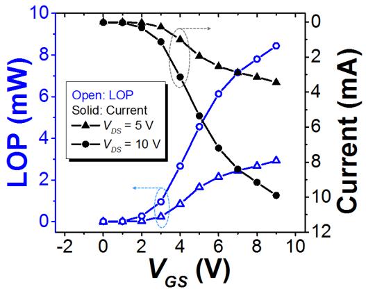
Figure 2: Gate modulated LOP and current–voltage characteristics of integrated VMOSFET-LED device at different drain biases.
The forward voltage at 20mA of the LED was 3.72V; the light output power and external quantum efficiency (EQE) at the same current were 16mW and 23.5%, respectively. Peak EQE (33%) was achieved at 600mA/cm2 current density (0.54mA). With a reverse bias of -10V, the leakage was 10-2mA. The blue LED wavelength peaked around 440nm.
The researchers comment: “The dramatic improvement in LED brightness compared to the previously reported integration schemes was mainly attributed to the better crystalline quality of LED epiwafer grown on pss than those grown on planar sapphire substrates.”
The VMOSFET had a positive threshold of +1.8V, giving desired normally-on ‘enhancement-mode’ operation. The maximum output current density was 1.4kA/cm2 with 11V drain bias and 9V gate potential. The team points out that a previous device produced without TMAH-solution etching had an order-of-magnitude lower output current density.
VMOSFET-LED integration allows simpler voltage control rather than current control of the light output. Below the threshold voltage of the VMOSFET there was no measured light output. With 9V gate (VGS) and 10V drain (VDS), the light output power (LOP) was 8.5mW (9.4W/cm2). The injection current through the transistor was 10mA.
The team writes: “To our knowledge, this is the best performance ever reported for monolithic integration of GaN LEDs with driving transistors. Nevertheless, the high VDS of the integrated VMOSFET-LED leads to a high power consumption. The drive voltage can be reduced by increasing the VMOSFET’s device size to improve its drive capability.”
GaN LEDs GaN LEDs Driving transistors
https://doi.org/10.1109/LED.2017.2691908
The author Mike Cooke is a freelance technology journalist who has worked in the semiconductor and advanced technology sectors since 1997.


