


- News
7 April 2017
Gallium nitride fin transistor with high linearity and output power
Nanjing Electronic Devices Institute in China has used fin structures to improve the linearity of aluminium gallium nitride/gallium nitride (AlGaN/GaN) high-electron-mobility transistors (HEMTs) [Kai Zhang et al, IEEE Electron Device Letters, published online 24 March 2017]. The team comments: “To the best of our knowledge, this is the first demonstration of superior power performance of high-linearity GaN finFETs, indicating significant advantages of tri-gate configuration over planar HEMTs for microwave power applications.”
Fin structures allow better electrostatic control of channel conduction by transistor gates, reducing the negative short-channel effects of the scaled gate-lengths needed for high-frequency operation. Linearity in radio frequency (RF) operation is also highly desired for mobile communication platforms.
An AlGaN/GaN epitaxial structure – a 16nm Al0.3Ga0.7N barrier, a 1nm AlN spacer, and a 1.5μm GaN buffer – was grown on silicon carbide (SiC), giving a two-dimensional electron gas with 1.06x10¹³/cm2 carrier density of 2170cm2/V-s mobility, according to Hall measurements.
Device fabrication began with alloyed titanium/aluminium/nickel/gold ohmic contact formation, argon ion implant for electrical isolation, and plasma-enhanced chemical vapor deposition (PECVD) of 100nm silicon nitride passivation.
A gate opening with 180nm gate-length footprint was made in the silicon nitride before 800nm-long nanowire patterns were etch down 30nm to completely remove the AlGaN/GaN channels between the wires. The fin width was 152nm. The period of the fin structures was 400nm.
The 0.9μm field-plate gate electrode was formed from nickel/gold. A further 250nm silicon nitride passivation layer was deposited, followed by gold air-bridge interconnections. The T-gate overhang was 0.36μm in both directions. The source-drain distance was 4.0μm.
The gate width and pitch were 2x125μm (250μm total) and 20μm, respectively. The number of fins in the field-effect transistor (FET) was 625 (250μm/400nm). The effective gate width was 95μm (625x152nm).
The maximum DC current density at 1V gate potential was 1.64A/mm, which was 1.45x that of a comparison planar HEMT. With 14V drain bias, planar HEMTs suffered from a 21% drop in current compared with pulsed operation, suggesting performance degradation due to severe self-heating. The drop at the same bias for the finFETs was 9%. “This remarkable improvement could be attributed to reduced thermal resistance in finFETs stemming from additional lateral heat spreading of sidewall gates,” the team comments.
Current collapse measurements using different quiescent/off states showed similar performance effects from charge trapping for fin and planar HEMTs.
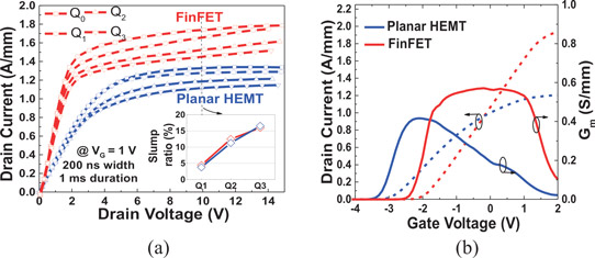
Figure 1: (a) Current dispersion and (b) DC transfer characteristics of planar HEMT and finFET measured at 10V drain bias.
Another effect of the fins is a positive shift in threshold of about 1V due to depletion effects on the fin sidewalls (Figure 1). Also, the transconductance (Gm) is near the maximum over a broader range than for planar HEMTs. Further, the finFET transconductance peak is higher than that of the planar device.
Gate leakage through the sidewalls of the finFET does impact on/off current ratio somewhat. The drain-induced barrier lowering (DIBL) was improved (35mV/V) over that of the planar device (68mV/V). The subthreshold swings (SSs) were similar. Improved off current, DIBL and SS could come from an optimized etching process, forming a steep fin shape, the team believes.
Small-signal radio frequency measurement resulted, respectively, in peak cut-off (fT) and maximum oscillation (fmax) frequencies of 31GHz and 78GHz for the finFET, and 45GHz and 92GHz for the planar HEMT.
The researchers comment: “As a result of incorporation of T-gate structure, the balanced fT/fmax values are achieved, indicating the proposed finFET with high-linearity Gm characteristics is suitable for microwave power applications. The relative lower frequency performance in finFET is mainly caused by additional parasitic capacitance originating from etched GaN region and sidewall gates.”
In 8GHz two-tone load-pull testing, the output power reached 11.3W/mm for the finFET, while the planar HEMT produced 6.8W/mm (Figure 2). The drain bias was 28V and the quiescent current was 10% of the maximum. While both devices had a similar power-added efficiency (PAE) of ~53%, the finFET showed improved linearity, with ~5.5dBc (decibels relative to carrier) less third-order intermodulation (IM3) distortion.
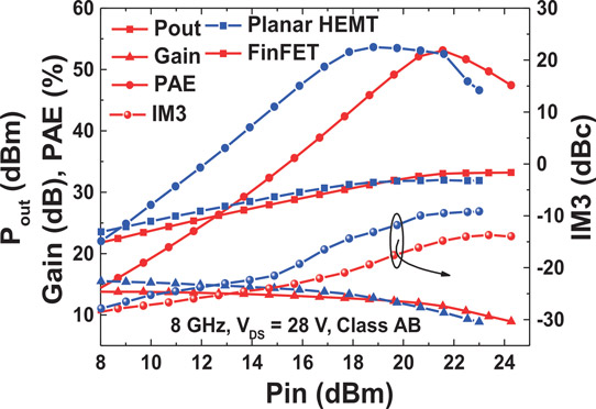
Figure 2: Two-tone power linearity characteristics of finFET and planar HEMT.
The researchers believe that scaling down the gate length would allow access to higher-frequency performance.
AlGaN/GaN HEMTs GaN FinFETs GaN SiC
https://doi.org/10.1109/LED.2017.2687440
The author Mike Cooke is a freelance technology journalist who has worked in the semiconductor and advanced technology sectors since 1997.


