


- News
19 April 2017
Improving vertical gallium nitride Schottky barrier diodes
National Institute for Materials Science (NIMS) in Japan and Shanghai University in China have developed vertical gallium nitride (GaN) Schottky barrier diodes (SBDs) with a combination of low turn-on voltage and low on-resistance [Bing Ren et al, Appl. Phys. Express, vol10, p051001, 2017]. The low turn-on voltages obtained are claimed to be “the lowest values ever reported for the vertical GaN SBD”.
The team used a lowered growth rate to improve the GaN drift layer. The researchers see the technique as a route to high-performance vertical GaN SBDs with low conduction loss and high switching speed suitable for high-power applications.
The vertical structure allows simultaneous high current and voltage with reduced on-resistance and less performance degradation from surface and interface states, compared with more conventional lateral devices. Progress to vertical technology has been enable by the fast development of free-standing GaN substrates with low threading dislocation density.
The GaN drift layer was grown by metal-organic chemical vapor deposition (MOCVD) at 950°C on free-standing substrates with 4x10⁶/cm2 threading dislocation density and 1x10¹⁸/cm3 donor concentration. The precursors were trimethyl-gallium (TMG) and ammonia (NH3) in a carrier gas that was a mix of nitrogen and hydrogen.
The growth rate was controlled by varying the TMG flow rate between 30 standard cubic centimeters (sccm) and 90sccm (Table 1). The ammonia flow was fixed at 10 standard liters per minute (slm), except for sample C. The NH3/TMG (V/III) molar ratio was between 1352 and 4057.
Table 1: Growth conditions, growth rate, root-mean-square (RMS) surface roughness, and thickness of grown GaN.
| Sample | TMG (sccm) |
NH3 (slm) |
V/III | Growth rate (μm/h) |
RMS (nm) |
Thickness (μm) |
| A | 30 | 10 | 4057 | 2.61 | 0.11 | 4.36 |
| B | 60 | 10 | 2028 | 4.72 | 0.62 | 7.95 |
| C | 90 | 15 | 2028 | 7.78 | 1.19 | 7.78 |
| D | 90 | 10 | 1352 | 8.08 | — | 8.08 |
Schottky barrier diodes were formed with sputtered titanium/aluminium/gold ohmic metals on the substrate back-side and evaporated nickel/gold as Schottky contact.
The researchers studied the surface of the grown GaN with atomic force microscopy (AFM). Samples A-C, grown with flow rates 2.6-7.81μm/h, had surfaces with aligned, atomic-level steps. By contrast, the 8.08μm/h fast growth rate of sample D resulted in valley-like defects. The researchers suggest that these defects could arise from a three-dimensional growth mode or from the relatively low V/III ratio.
The researchers comment: “Although the step-flow growth was achieved in an optimized growth rate range, the RMS roughness was still rising from 0.11 to 1.19nm with increasing growth rate.”
X-ray analysis produced rocking curves with similar narrow peaks with full-width at half-maximum (FWHM) values similar to that of the underlying substrate. Photoluminescence measurements showed sharp 3.4eV near-band-edge emission and broad ~2.2eV defect-related ‘yellow’ luminescence. The ratio of near-band-edge to yellow emissions trended downward with growth rate – around 60 for the bulk GaN substrate, and in the range 30-5 for samples A-D. The researchers attribute this to increased carbon incorporation, presumably from the organic TMG precursor. The low carbon incorporation of samples A and B improved the mobility of the SBD drift layer.
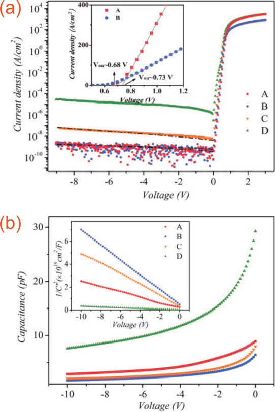
Figure 1: (a) Current density versus voltage and inset detail near turn-on point for samples A and B. (b) Capacitance-voltage measurements at 1MHz and inset inverse-square capacitance versus voltage.
Electrical characteristics (Figure 1 and Table 2) were extracted from SBDs with 60μm-diameter contacts. “Although the SBD devices have large Schottky barrier heights, the turn-on voltages were still kept at a low level (0.66–0.73V), which are the lowest values ever reported for the vertical GaN SBD,” the team writes.
The SBD based on sample A material gave a combination of low 0.72Ω-cm2 specific on-resistance and high 1370cm2/V-s mobility, at the cost of a slightly higher turn-on voltage compared with the other devices. Sample A’s on-resistance is described as “among the lowest ever reported”. “It should be noted that this is the first report of such a low on-resistance together with a low turn-on voltage,” the researchers add.
Table 2: Key diode parameters extracted from current-voltage (I–V) and capacitance-voltage C–V curves.
| Sample | n | φ I-V (eV) |
φ C-V (eV) |
Free carrier density (/cm3) |
Von (V) |
Ron (mΩ-cm2) |
Mobility [cm2/V-s] |
| A | 1.04 | 0.97 | 0.97 | 6.35x10¹⁵ | 0.73 | 0.72 | 1370 |
| B | 1.03 | 0.93 | 0.95 | 2.30x10¹⁵ | 0.68 | 2.62 | 975 |
| C | 1.04 | 0.85 | 0.91 | 3.10x10¹⁵ | 0.66 | 2.90 | 628 |
| D | 1.59 | 0.69 | 0.71 | 4.59x10¹⁶ | 0.67 | 0.86 | 239 |
The sharpness of the turn-on, as given by the ideality, is close to 1 (the ideal) for SBDs on samples A-C. The higher 1.59 ideality of sample D is attributed to the poor Schottky contact of the rough surface. Also, SBD sample D suffered from a higher reverse bias leakage of 105A/cm2, due to trap-assisted tunneling, according to the researchers. The Schottky barrier heights (φ) from current-voltage and capacitance-voltage analysis of the devices on samples A and B are close to the nickel/GaN theoretical value of 1.0eV.
GaN Schottky barrier diodes MOCVD
https://doi.org/10.7567/APEX.10.051001
The author Mike Cooke is a freelance technology journalist who has worked in the semiconductor and advanced technology sectors since 1997.


