


- News
23 August 2017
High-breakdown slanted tri-gate gallium nitride power transistors
Jun Ma and Elison Matioli of the École Polytechnique Fédérale de Lausanne in Switzerland have used slanted tri-gate structures to enhance the breakdown voltage of gallium nitride (GaN) metal-oxide-semiconductor high-electron-mobility transistors (MOSHEMTs) by 500V [IEEE Electron Device Letters, published online 25 July 2017]. They claim a record 1.2GW/cm2 high-power figure of merit.
The fabricated transistors (Figure 1) consisted of etched nanowires with slanted width within the gate region. The etch depth was 160nm into the aluminium gallium nitride (AlGaN) barrier on gallium nitride channel on silicon structure. The slant gave a 350nm width on the source side and 700nm on the drain side.
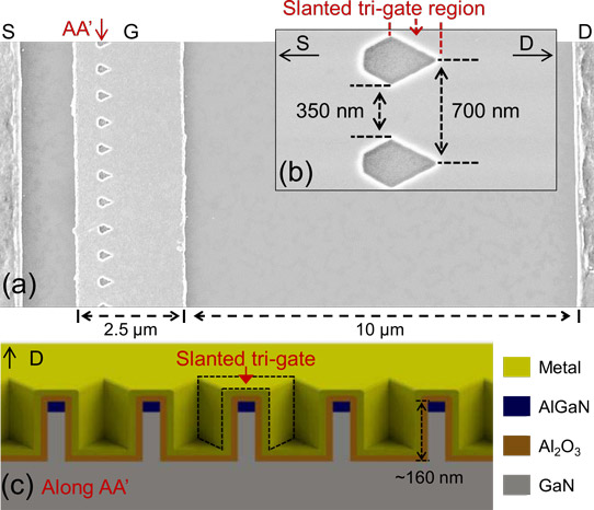
Figure 1: Scanning electron microscope top-view of slanted tri-gate MOSHEMT (a) with and (b) without gate dielectric and metal. (c) Cross-sectional schematic of slanted tri-gate along arrow AA’.
The gate stack consisted of 20nm atomic layer deposition (ALD) aluminium oxide (Al2O3) and metal wrapped around the channel. The source and drain planar sides of the gate were 0.5\micron and 1.5\micron, respectively. The total gate length was 2.5\micron. The source-gate and gate-drain distances were 1.5\micron and 10\micron, respectively.
Since the researchers were interested in the raw effect of slant gates, they did not use conventional field plates or passivation. In fact, the team sees the tri-gate structure as converting the planar part of the gate towards the drain side into an effective field plate. The slant structure allows the pinch-off potential to vary in such a way that the electric field is kept below critical. The varying potential is mainly achieved by strain relaxation in the AlGaN/GaN nanowires along with the increased electrostatic control offered by the sidewall gates of the tri-gate structure.
Without field plates, or the slant tri-gate structure, the electric field tends to peak at the gate edge on the drain side. However, while field plates require complex processing, tri-gates can be achieved with just one extra etch step.
Even introducing an unslanted tri-gate into the planar transistor improved the breakdown voltage from 877V to 1100V with a 1microA/mm leakage criterion. Slanting the tri-gates increased the breakdown further to 1350V, close to the buffer limit, even with a gate-drain distance as low as 10\micron.
The off leakage current (IOFF) at lower drain biases were higher in the slanted tri-gate structure, compared with the planar and unslanted tri-gate MOSHEMTs. The researchers comment: “The larger IOFF of the slanted tri-gate device at small voltages is likely due to its much smaller effective gate length, since the three devices have the same buffer leakage current as they were fabricated on the same chip, and exhibited small gate leakage currents ≤ 2nA/mm at 750V.”
The leakage dependences on bias voltage were similar above 750V up to near the respective breakdowns.
Beyond breakdown characteristics, the slanted tri-gate structure also exhibited a high on/off current ratio of more than 109 and high transconductance up to 72mS/mm at 5V drain bias. The transconductance of the planar device was lower, at 66mS/mm. The on-resistance of the devices was similar, at about 9\Ohm-mm.
The researchers also compared the slanted tri-gate device with transistors produced by other groups (Figure 2). They point out that their breakdown voltage was comparable with the best reported value of 1460V. At the same time, the specific on-resistance (RON,SP) was 3.6x lower due to the 14\micron shorter gate-drain distance in the slanted tri-gate MOSHEMT.
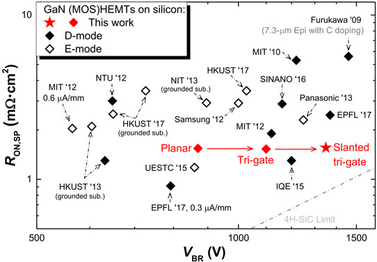
Figure 2: RON,SP versus VBR benchmark of slanted tri-gate MOSHEMTs against state-of-the-art GaN enhancement-mode and depletion-mode (MOS)HEMTs on silicon with breakdown criterion of 1\microA/mm. RON,SP based on 1.5\micron transfer length for each ohmic contact. VBR for all reference devices re-calculated based on 1\microA/mm criterion.
A widely used power transistor figure of merit, VBR2/RON,SP, was 1.2GW/cm2, claimed as a record value.
https://doi.org/10.1109/LED.2017.2731799
The author Mike Cooke is a freelance technology journalist who has worked in the semiconductor and advanced technology sectors since 1997.


