


- News
30 August 2017
Gallium nitride on silicon in-plane gate field-effect transistors
Giovanni Santoruvo and Elison Matioli of École Polytechnique Fédérale de Lausanne in Switzerland have combined in-plane gate field-effect transistors (IPGFETs) with gallium nitride (GaN) on silicon technology with a view to high-frequency power applications [IEEE Electron Device Letters, published online 9 August 2017]. The IPGFET (Figure 1) uses gate electrodes etched from the same level as the channel to control current flow. There is no need for dielectrics since the gate is insulated from the channel by air.
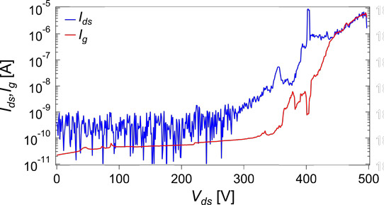
Figure 1: (a) Schematic and (b) top-view scanning electron microscope (SEM) image of 165nm-wide, 250nm-long IPGFET. Zoomed top-view SEM of 250nm-long (c) and 50nm-long (d) IPGFETs.
Santoruvo and Matioli comment: “High-frequency devices require a small gate capacitance in addition to a large gm [transconductance], which is an intrinsic advantage of IPGFETs.”
Although IPGFETs have been realized in other compound semiconductor materials, Santoruvo and Matioli claim that their work is the first to use III-nitrides to produce high-performance IPGFETs. III-nitride should enable access to high carrier density and high breakdown voltages.
The III-nitride semiconductor material consisted of silicon substrate, 3.75µm GaN buffer, 300nm GaN channel, 8nm aluminium nitride (AlN) spacer, and 23.5nm Al0.25Ga0.75N barrier. The two-dimensional electron gas formed at the top GaN interface with the spacer/barrier had 1.05x10¹³/cm2 carrier concentration, 1690cm2/V-s mobility, and 350Ω/square sheet resistance.
The channel, source, drain and gate were fabricated using electron-beam lithography and inductively coupled plasma etch. Devices with varying parameters were defined. Annealed ohmic contacts to the source, drain and gate consisted of titanium/aluminium/titanium/nickel/gold.
This essentially two-step fabrication results in transistors with self-aligned gates. No insulation oxides or passivation layers were used. Such additions to improve performance are suggested as future work by Santoruvo and Matioli.
Wide-channel devices had larger maximum drain current and threshold voltage magnitude. The devices were normally-on, so the threshold was negative. The wider channels naturally had lower resistance. However, the narrower-channel devices had a further effect increasing resistance – strain relaxation in the AlGaN barrier, decreasing carrier density due to reduced piezoelectric effects. Reducing the channel length also reduced resistance, giving similar increases in drain current and threshold.
The on/off current ratio was of the order 107 with less than 10pA leakage current for 210nm deep trench etching. Shallower trench etching to 140nm gave a slightly higher leakage, but still less than 100pA.
The shallower trenches also gave devices with more positive thresholds – i.e. the magnitude was smaller. This is attributed to an increase in gate capacitance for the shallower trenches.
Santoruvo and Matioli estimate the total effective capacitance of 0.7-3.9aF (where aF = atto-Farads = 10-18F) for deep IPGFETs of widths 20-85nm. The corresponding values for shallow transistors were in the range 2.2-9.4aF. “These are extremely small values of gate capacitance, which are very promising for high-frequency applications,” the researchers comment.
On the basis of these values, they estimate potential for up to 0.89THz cut-off frequencies, although the reported devices were not designed or tested for high-frequency performance.
A 50nm-long, 85nm-wide shallow IPGFET achieved a drain current of 1.4A/mm, which is 9x the value reported for similar structures using indium gallium arsenide (InGaAs) quantum well material. The improvement for GaN IPGFETs is credited to much larger carrier densities and very small sidewall depletion in III-nitrides.
Shallow 50nm-channel-length IPGFETs also demonstrated higher transconductance, which increased over a broader range of gate potentials with channel width. Normalized by channel width, the peak transconductance was 335mS/mm for 85nm-wide channels and 665mS/mm for 20nm. The latter value is 5x that of previous reports. The increase in normalized transconductance for narrower channels is attributed to improved modulation by the gate.
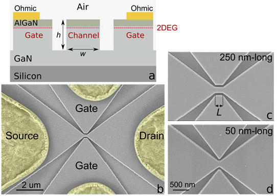
Figure 2: Drain and gate currents for 165nm-wide, 250nm-long IPGFET in -11V gate off-state.
In the -11V gate potential ‘off’ state, leakage was maintained at a low level up to 300V (less than 1nA drain and 100pA gate current), breaking down at 500V (Figure 2). This performance trend was independent of channel width. “The similar behavior of Ids and Ig suggests that at large voltages the leakage current flows entirely through the semiconductor buffer layers, not through the nanowires, since both the drain and gate contacts are ohmic,” Santoruvo and Matioli write.
https://doi.org/10.1109/LED.2017.2737658
The author Mike Cooke is a freelance technology journalist who has worked in the semiconductor and advanced technology sectors since 1997.


