


- News
21 August 2017
NIMS develops logic circuit with both D- and E-mode diamond-based MOSFETs
A research group at Japan’s National Institute for Materials Science (NIMS) led by Jiangwei Liu (independent scientist, Research Center for Functional Materials) and Yasuo Koide (coordinating director in the Research Network and Facility Services Division) has developed (for the first time, it is reckoned) logic circuits equipped with diamond-based metal-oxide-semiconductor field-effect-transistors (MOSFETs) at two different operation modes - a first step toward the development of diamond integrated circuits operational under extreme environments (Liu et al, ‘Logic Circuits With Hydrogenated Diamond Field-Effect Transistors’, IEEE Electron Device Letters vol38, issue 7, p922-925).
Since it has high carrier mobility, a high breakdown electric field and high thermal conductivity, diamond is a promising material for the development of current switches and ICs required to operate stably at high temperature, high frequency and high power. However, it had been difficult to enable diamond-based MOSFETs to control the polarity of the threshold voltage, and to fabricate MOSFETs of two different modes ― depletion mode (D mode) and enhancement mode (E mode) ― on the same substrate. The research group has developed a logic circuit equipped with both D-mode and E-mode diamond MOSFETs after fabricating them on the same substrate using a threshold control technique developed by the group.
The researchers identified the electronic structure in the interface between various oxides and hydrogenated diamond using photoelectron spectroscopy in 2012. Then, after many difficulties, in 2013 the group then developed a diamond metal-oxide-semiconductor (MOS) capacitor with very low leakage current density and an E-mode hydrogenated diamond-based MOSFET. In 2014, the group then prototyped logic circuits by combining diamond-based MOSFETs with load resistors. Finally, in 2015, the group developed techniques to control D- and E-mode characteristics of diamond-based MOSFETs and identified the control mechanism.
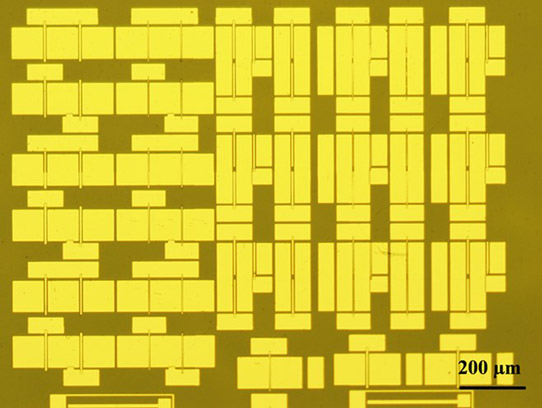
Picture: Micrograph of logic circuit with diamond-based transistors.
The new logic circuits with diamond-based transistors are reckoned to be promising for the development of digital ICs that are required to operate stably under extreme environments, such as at high temperature as well as under exposure to radiation and cosmic rays.
The research was conducted in conjunction with the following projects: Leading Initiative for Excellent Young Researchers (Jiangwei Liu, representative), under the sponsorship of the MEXT Human Resource Development Program for Science and Technology; ‘Development of new functional diamond electronic devices using a large amount of polarized charges’ (with principal investigator Yasuo Koide) under the category of Grant-in-Aid for Scientific Research (A) sponsored by the MEXT Grants-in-Aid for Scientific Research; and ‘Fabrication of high-current-output fin-type diamond field-effect transistors’ (with principal investigator Jiangwei Liu) under the category of Grant-in-Aid for Young Scientists (B) sponsored by the MEXT Grants-in-Aid for Scientific Research. Device fabrication was supported by the NIMS Nanofabrication Platform, established under the MEXT Nanotechnology Platform Japan program.
http://dx.doi.org/10.1109/LED.2017.2702744


