


- News
11 December 2017
Disco’s KABRA!zen fully automates KABRA laser slicing technology
© Semiconductor Today Magazine / Juno Publishing
At SEMICON Japan at Tokyo Big Sight (13-15 December), Tokyo-based equipment maker Disco Corp is exhibiting KABRA!zen, which introduces fully automatic transfer between the stages of its KABRA (Key Amorphous-Black Repetitive Absorption) laser-based ingot slicing process for silicon carbide (SiC).
Since there will be an increase in electric power consumption across a wide range of products due to the development of the Internet of Things (IoT) and the use of electronics in vehicles, there is expected to be widespread use of energy-saving power devices that use next-generation materials such as SiC. However, in the conventional diamond wire saw ingot slicing method, low throughput and a large amount of material loss during processing has been causing an increase in manufacturing costs.
In the KABRA slicing process, by continuously irradiating the laser vertically from the upper surface of the ingot, a separating layer that absorbs light is formed into a flat shape at the desired depth, enabling peeling and formation of wafers from this point.
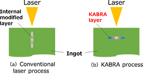 Picture: The KABRA process versus a conventional laser slicing process.
However, because the existing KABRA process requires an operator to remount workpieces before each process (including laser irradiation, wafer separation, fine grinding down to the designated thickness, and grinding of the top surface of the ingot), throughput was affected by the operator’s ability.
In contrast, KABRA!zen fully automates transfer between each stage of the KABRA process (all unmanned). Consequently, throughput has been improved by about 50% (for 350µm-thick wafers produced from a 6”-diameter, 40mm-thick SiC ingot). This further accelerates the advances being made in SiC wafer production efficiency, says Disco.
Also, because the system connects each of the laser, separation and grinding processes, the number of machines used for each process can be customized according to the various criteria, such as the number of wafers produced, surface finish condition, etc.
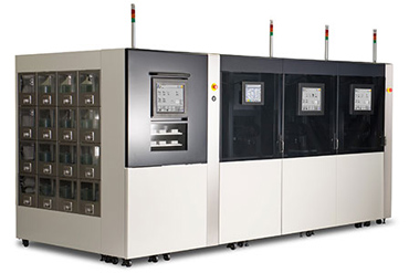 Picture: Figure 2: The KABRA!zen system, as exhibited at SEMICON Japan (configured to perform the KABRA process using the minimum amount of equipment).
Disco has 53 patents (issued and pending) related to KABRA, including 13 process-related patents, 3 full automation (KABRA!zen) patents, 19 laser irradiation patents, 7 separation patents, 2 grinding patents, plus 9 miscellaneous patents.
The firm says that it has already received inquiries regarding KABRA!zen from major wafer manufacturing companies, and is aiming to ship test equipment in 2018. Full automation is also possible by retrofitting existing equipment, e.g. the preceding, manual DAL7420 KABRA system.
Disco develops laser ingot slicing method to speed SiC wafer production and cut material loss


