


- News
18 December 2017
Fujitsu bonds single-crystal diamond and SiC substrate at room temperature, boosting GaN HEMT performance
© Semiconductor Today Magazine / Juno Publishing
At the IEEE Semiconductor Interface Specialists Conference (SISC2017) in San Diego, CA, USA (6-9 December), Fujitsu Ltd and its subsidiary Fujitsu Laboratories Ltd presented what is claimed to be the first technology for room-temperature bonding of single-crystal diamond to a silicon carbide (SiC) substrate, which are both hard materials but with different coefficients of thermal expansion.
Using this technology for heat dissipation allows high-efficiency cooling of high-power gallium nitride (GaN) high-electron-mobility transistors (HEMTs), enabling stable operations of power amplifiers at high power levels.
In recent years, high-frequency GaN-HEMT power amplifiers have been widely used for long-range radio applications, such as radar and wireless communications. They are also expected to be used in weather radar observing localized heavy rains, for example, or in the forthcoming 5G millimeter-band mobile communications protocols. For these types of radars or wireless communications using the microwave to millimeter-wave bands, by raising the output of the GaN-HEMT power amplifiers used for transmission, the distance that radio waves can propagate will allow the expansion of the observational range of radar while enabling longer and higher-capacity communications.
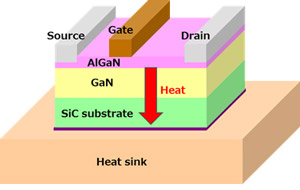 Graphic: Structure of conventional GaN HEMT power amplifier.
In GaN-HEMT power amplifiers, some of the input power is converted to heat (Figure 1), which is dispersed into the SiC substrate. Since boosting the range and power in radar and wireless communications also increases the heat produced by devices, this adversely affects their performance and reliability, creating a need to efficiently carry device heat to a cooling structure (heat sink).
Although the SiC substrate has relatively high thermal conductivity, a material with even better thermal conductivity is needed for devices with increasingly higher power output to efficiently carry device heat to the cooling structure. Single-crystal diamond has extremely good thermal conductivity - almost five times that of a SiC substrate - and is known as a material that can efficiently spread heat.
To bond a single-crystal diamond to a device as a cooling material, normal production processes use an argon (Ar) beam to remove impurities. However, this creates a low-density damaged layer on the surface, which weakens the bonds that the single-crystal diamond can form. Also, using an insulating film such as silicon nitride (SiN) for bonding impairs the thermal conductivity due to the thermal resistance of SiN.
To prevent the Ar beam from forming a damaged layer on the diamond surface, Fujitsu has developed a technique that protects the surface with an extremely thin metallic film before it is exposed to the Ar beam (see Figure 2). To ensure that the surface is planar (for good bonding at room temperature), the metallic film’s thickness is limited to 10nm or less.
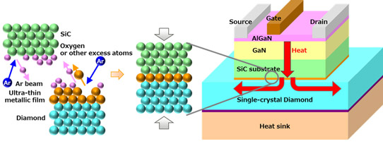
Graphic: Structure of GaN HEMT power amplifier with bonded diamond.
This technology was confirmed to prevent the formation of the damaged layer on the diamond surface after Ar beam exposure (Figure 3), resulting in improved bonding strength and hence single-crystal diamond bonded at room temperature to a SiC substrate.
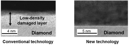
Figure 3: Diamond cross section after Ar beam exposure.
Thermal resistance was measured in samples bonded at room temperature, and the SiC/diamond interface was found to have an extremely low thermal resistance of 6.7×10⁻⁸m2K/W. Simulations using this measured parameter show that this technology would significantly reduce the thermal resistance of 200W-class GaN-HEMT devices, to 61% that of existing devices (equivalent to an 80°C reduction in surface temperature) - see Figure 4.
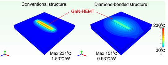
Figure 4: Simulated comparison of heat in 200W-class GaN HEMT power amplifiers.
Use of this technology hence promises to yield GaN-HEMT power amplifiers for transmitters with even higher power output. When used in systems such as weather radars, GaN-HEMT power amplifiers for transmitters can be expected to increase the radar’s observable range by a factor of 1.5. This would allow quicker detection of the cumulonimbus clouds that can produce sudden rainstorms, contributing to greater disaster readiness, says Fujitsu.
Fujitsu plans to assess the thermal resistance and output performance of GaN-HEMTs using this technology, aiming to implement it in high-output, high-frequency power amplifiers in fiscal 2020, for application in weather radar and 5G wireless communications systems.
The research was conducted in part with support from the Innovative Science and Technology Initiative for Security, established by the Acquisition, Technology & Logistics Agency (ALTA) of Japan’s Ministry of Defense.
www.fujitsu.com/jp/group/labs/en


