


- News
7 December 2017
Gallium nitride transistor on silicon with 250GHz cut-off frequency
Researchers based in Singapore and USA claim the highest cut-off frequency so far for gallium nitride (GaN) high-electron-mobility transistors (HEMTs) produced on silicon (Si) substrates [Weichuan Xing et al, IEEE Electron Device Letters, published online 13 November 2017]. The devices with indium aluminium nitride (InAlN) barrier layer and gate length of 40nm achieved a cut-off of 250GHz.
The performance compares well with GaN HEMTs produced on silicon carbide (SiC) substrates, which have smaller diameter and are much more expensive. Si-based production methods could open up many commercial opportunities. The III-nitride material system with its wide bandgaps enables higher breakdown fields and high electron saturation velocity with potential applications for high-frequency and high-power performance. The researchers estimate that their devices achieved 1.1x107cm/s electron saturation velocity.
“The next generation of communication systems, including 5G, vehicles and Internet of Things, needs devices operating at mm-wave bands with low cost and high-efficiency”, comment the researchers from Singapore’s Nanyang Technological University, Singapore-MIT Alliance of Research and Technology, Temasek Laboratories Singapore, and Massachusetts Institute of Technology in the USA. The 1cm to 1mm range of wavelengths covers frequencies from 30GHz to 300GHz.
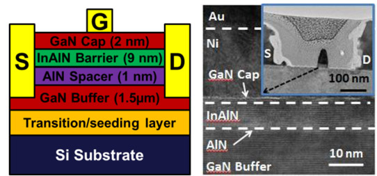
Figure 1: Schematic and transmission electron microscope (TEM) image (gate region) of 40nm gate InAlN/GaN on Si.
The epitaxial structure (Figure 1) was grown by metal-organic chemical vapor deposition (MOCVD) on (111) silicon with high-resistivity greater than 6000Ω-cm. High-resistance substrates are preferred in high-frequency applications to avoid energy losses from induced current flows. The InAlN barrier layers was lattice matched with 17% indium content. Hall measurement gave a carrier concentration of 2.04x10¹³/cm2 in the two-dimensional electron gas that forms in the GaN channel near the GaN/AlN/InAlN interface. The mobility was 1190cm2/V-s. The AlN spacer was designed to screen channel-electron scattering from the barrier, improving electron mobility.
Mesa isolation for transistor fabrication was achieved with 120nm-deep plasma etching. The ohmic source and drain contacts consisted of annealed titanium/aluminium/nickel/gold. The rectangular gate was nickel/gold. Further metalization for interconnects and probe pads consisted of titanium/gold. Initially, there was no surface passivation.
The source-drain distance was 300nm for the shortest 40nm gate-length transistor. Longer gates were accommodated in a 700nm gap. The gate width was 2x50μm (100μm total).
The maximum drain current of the 40nm-gate device was 2.66A/mm with 2V gate and 6V drain bias. The peak transconductance was 438mS/mm at -2.8V gate and 6V drain voltage points. Reported III-nitride devices on SIC substrates have achieved similar drain currents, but slightly higher transconductance (520mS/mm). The researchers point to two factors that give the SiC-based device the edge: a higher mobility of 1581cm2/V-s, and a thinner total barrier thickness of 9.4nm. The barrier for the silicon-based contender consisted of 2nm GaN cap, 9nm InAlN, and 1nm AlN spacer, giving a 12nm total.
The gate leakage (Ig) was high, exceeding 1mA/mm with -10V gate. “The high Ig is due to the thin InAlN barrier and the high peak electrical field in the deeply scaled gate HEMT,” the team comments.
Frequency measurements gave a cut-off (fT) of 250GHz and maximum oscillation (fmax) of 60GHz. The researchers comment: “To the best of our knowledge, this fT value is the highest among the reported GaN-based transistors on Si substrates. A relatively low fmax is due to the high resistance of the short rectangular-shape gate, which can be improved by using T-shape gate structure.” They also suggest that “fin-like or planar nano-channels under the gate” could improve linearity.
To reduce current collapse, the researchers applied surface passivation consisting of 10nm aluminium oxide from an atomic layer deposition (ALD) process. The collapse under pulsed operation was reduced from 90% to 15% with a -8V gate and 6V drain quiescent state. At 0V drain and -8V gate quiescent, the collapse decreased from 85% to 5% by adding passivation. The penalty of passivation was that fT fell to 235GHz. The researchers suggest a low-k passivation could restore the frequency performance.
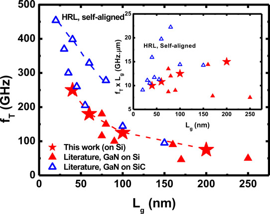
Figure 2: Comparison of fT of GaN HEMTs on Si in Xing et al’s work with other reported GaN HEMTs on Si and on SiC. Inset: gate-length (Lg) dependence of fT x Lg product.
Longer-gate devices had lower fT values: 75GHz, 125GHz and 180GHz for respective gate lengths of 200nm, 100nm and 60nm. In 2013 HRL reported a 454GHz fT for an AlN/GaN HEMT on SiC. Other reports of GaN on SiC have similar frequency performance to Xing et al’s HEMT on Si (Figure 2). “These excellent results show the great potential of InAlN/GaN HEMTs on Si for future mm-wave and sub-THz applications”, the team writes.
The researchers also suggest that reducing the gate length further to 20nm and adopting a self-aligned process as in HRL’s device could lead to performance improvement. The team’s analysis suggests an fT of 440GHz could be accessed with 20nm gate, 150nm source-drain distance, and regrown n++-GaN ohmic contacts.
GaN HEMTs GaN Silicon substrates MOCVD
https://doi.org/10.1109/LED.2017.2773054
The author Mike Cooke is a freelance technology journalist who has worked in the semiconductor and advanced technology sectors since 1997.


