


- News
8 February 2017
Gallium nitride quantum dot emission at 232nm deep ultraviolet
Cornell University and University of Notre Dame in the USA have claimed the shortest-wavelength electroluminescence so far using gallium nitride (GaN) active material [S. M. Islam et al, Appl. Phys. Lett., vol110, p041108, 2017]. The use of quantum dot (QD) structures and charge polarization effects to improve doping effectiveness allowed the team to achieve wavelengths as short as 232nm in the deep ultraviolet (UV in the 100-280nm C-band).
Efficient short-wavelength light-emitting diodes (LEDs) would lead to environmentally friendly, compact/portable alternatives to mercury lamps. Such UV LEDs are proposed for use in water purification, medical diagnostics, and security.
However, efficiency in UV LEDs based on III-nitride materials such as wide bandgap aluminium gallium nitride (AlGaN) falls steeply when wavelengths are reduced below 240nm. The Cornell/Notre Dame approach combined the confinement of electrons and holes in 'zero-dimension' QDs, increasing the bandgap from GaN's bulk value of 3.4eV, and boosting carrier injection into the active light-emitting region.
The team comments: "The reduced dimensionality of the active region can also be suitable for amplified spontaneous emission for LEDs and perhaps lower the threshold for realizing electrically injected deep-UV Lasers, which remains an unsolved problem in semiconductor physics."
Hole injection is a particular problem in III-nitrides. Already in GaN the activation energy for magnesium doping is ~200meV, while room temperature thermal effects are around 26meV. This means that the ionization rate is very low and hole densities are poor. The activation energy increases as aluminium is added to widen the bandgap of AlGaN for shorter-wavelength emission. The Cornell/Notre Dame team improved ionization rates by using the differing charge polarization of the III-nitride bond with graded-Al-content AlGaN.
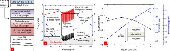
Figure 1: (a) Heterostructure layer design of deep-UV LED, (b) simulated energy band diagram at 5V forward bias, and (c) calculated evolution of UV emission wavelength and wavefunction overlap integral with GaN ML thickness.
Plasma molecular beam epitaxy (MBE) created deep UV heterostructures on metal-polar AlN/sapphire templates (Figure 1). The active region consisted of layers of GaN QDs of 1 to 4 monolayers (MLs) thickness in AlN barrier material. The AlN barrier layers were created by depositing 8 monolayers of Al without nitrogen, followed by nitrogen without Al, in a migration-enhanced epitaxy (MEE) process.
Lateral 200μmx200μm LEDs were produced using chlorine-based reactive ion etch of the mesa. The n- and p-type metal electrodes were titanium/aluminium/nickel/gold and titanium/gold, respectively. A thin nickel/gold current-spreading layer was applied to the p-contact before the p-electrode.
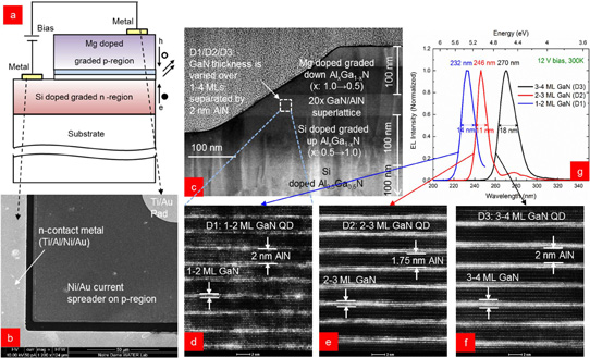
Figure 2: (a) Schematic of processed device and (b) scanning electron micrograph (top view quadrant) of processed device showing n and p metal contacts. (c) High-angle annular dark-field (HAADF) scanning transmission electron microscopy (STEM) image showing different layers for typical sample (D1/D2/D3), and zoomed in active region for (d) D1, (e) D2, (f) D3, along with (g) electroluminescence spectra taken at 12V forward bias for D1–D3 at 300K.
Electroluminescence peaks were observed at 270nm (4.59eV), 246nm (5.04eV) and 232nm (5.34eV)) under 10kHz/5% duty cycle pulsed 12V operation (Figure 2). The shortest wavelength was for 1-2ML QDs (D1). The other devices were based on 2-3ML (D2) and 3-4ML (D3) QDs.
The current densities were 165A/cm2, 90A/cm2 and 290A/cm2 for the 270nm, 246nm and 232nm peak-wavelength devices, respectively. The turn-on voltage for the devices was around 7.5V. The higher-than-expected turn-on voltage was blamed on poor p-contacts and a non-optimum number of 20 active region layers.
The team reports: "Based on some recent simulation and experimental work, 8 periods of the active region seem to be the optimum in terms of the light output and forward voltage drop across the device. Reducing the number of periods and further improvements in the p-layer design using tunnel-contacts can potentially help improve the hole injection problem for deep-UV LEDs."
There was some discrepancy with simulated emission peaks that the researchers attribute to inhomogeneous quantum dot distributions and quantum well and barrier thickness variations, along with uncertainties in the conduction and valence band structure. In particular, the linewidth was broader in reality, compared with simulations.
The researchers comment: "The shortest EL wavelength reported so far using the GaN active region is 239nm by metal-organic chemical vapor deposition (MOCVD) and 243nm by MBE. This work demonstrates that, by changing the thickness of the GaN layer with a ML precision, it is possible to achieve tunable deep UV LEDs emitting as short as 232nm."
Logarithmic plots of the emissions were used to study secondary peaks due to absorption and re-emission at longer wavelength of photons by lower-Al-content AlGaN in the magnesium-doped p-contact region. The Al-content was graded between 100% and 50% in order to increase hole carrier injection into the active region through charge polarization doping enhancement. Both the 1-2ML and 2-3ML had secondary peaks around 4.6eV photon energy, corresponding to the bandgap of Al0.5Ga0.5N. By contrast, there is no secondary peak for 3-4ML QD emissions since Al0.5Ga0.5N is transparent to 270nm UV.
http://dx.doi.org/10.1063/1.4975068
The author Mike Cooke is a freelance technology journalist who has worked in the semiconductor and advanced technology sectors since 1997.


