


- News
20 February 2017
Bulk aluminium nitride platform for gallium nitride high voltage and power
University of Notre Dame and Cornell University in the USA have claimed the first measurements on aluminium nitride/gallium nitride (AlN/GaN/AlN) quantum well (QW) field-effect transistors (FETs) on bulk AlN substrates with re-grown ohmic contacts [Meng Qi et al, Appl. Phys. Lett., vol110, p063501, 2017]. A device with 65nm gate length achieved a record-high drain current of 2A/mm, it is claimed. The researchers see potential for future high-voltage and high-power microwave electronics.
The use of AlN increases the bandgap to 6.2eV, while a large conduction band offset increases the electron confinement in GaN QWs. The GaN/AlN charge polarization contrast should also increase carrier densities and drive currents.
Another attractive feature of AlN is a high thermal conductivity of 340W/m-K, which is close to that of silicon carbide substrates (370W/m-K), which are often used for state-of-the-art AlGaN/GaN devices. High thermal conductivity relieves heat dissipation in high-power operation.
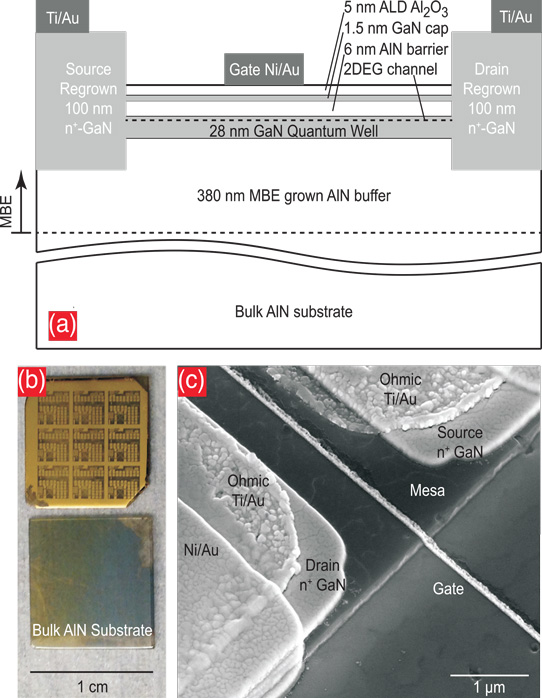
Figure 1: (a) Schematic cross-section layer structure of AlN/GaN/GaN heterostructure FETs on bulk AlN substrates (not to scale). (b) Images of grown and processed sample (top), and unprocessed bulk AlN substrate (bottom). (c) SEM image of finished short-gate-length GaN quantum well FET.
The AlN/GaN/AlN quantum well structures (Figure 1) were grown by radio frequency plasma molecular beam epitaxy (MBE) on semi-insulating aluminium-polar bulk AlN substrates. The wafers were 400μm thick. The structure also included a 1.5nm GaN cap to prevent oxidation of the 6nm AlN top barrier.
The conductivity of the two-dimensional electron gas (2DEG) that forms near the AlN/GaN QW interface through charge polarization effects was characterized by Hall measurements, giving a sheet carrier density (ns) of 2.8x10¹³/cm2, a mobility (μ) of 260cm2/V-s, and sheet resistance (Rsh) of 835Ω/square.
The researchers did produce a structure with 601cm2/V-s μ, 3.2x10¹³/cm2 ns, and 327Ω/square Rsh. In that case the GaN layer was 21nm, and the AlN top barrier was 3nm. The improved performance is attributed to modified nucleation conditions in the epitaxy process. Referring to these figures, and measurements carried out at 77K, the researchers comment: "These are the highest measured mobility and lowest sheet resistance for the AlN/GaN/AlN strained quantum well heterostructures on the AlN platform till date."
Unfortunately, the team was unable to capitalize on the structure due to fabrication difficulties and limited supply of substrate material. In particular, there was a lithography alignment problem. The team is presently attempting to more fully understand the transport properties of the AlN/GaN/AlN structure and the reason why the mobility is lower than for structures on GaN substrates.
Short-channel FET fabrication consisted of 40nm reactive-ion etch and MBE re-growth of n+-GaN as the source-drain contacts with titanium/gold electrodes, atomic layer deposition (ALD) of 5nm aluminium oxide (Al2O3) and deposition of nickel/gold gates. Nickel/gold was also added to the source-drain electrodes. The researchers also produced long-channel devices where the gate metals were deposited on the GaN cap, followed by 5nm ALD of Al2O3.
Raman spectroscopy indicated that the compressive strain of the channel was almost completely relaxed in the re-grown GaN of the source-drain contacts. Hall measurements on the FET structure gave 3.4x10¹³/cm2 ns, 180cm2/V-s μ, and 1020Ω/square Rsh. The researchers comment that the reduced μ and increased Rsh "from the as-grown sample may be due to the modification of surface states by the ALD Al2O3 layer." Transmission line structure measurements gave a specific contact resistance of 0.13Ω-mm and sheet resistance of 1100Ω/square.
The short-channel device demonstrated 2A/mm current density at 12V drain and +1V gate bias, 3x higher than for the long-channel FET. The short-channel FET had 65nm gate length and 2x50μm width. The gate-source and source-drain distances were 170nm and 850nm, respectively. The long-channel parameters were 1μm gate length, 50μm width, 1.5μm source-gate, and 5μm source-drain.
An 80nm gate-length FET had increased current density of 2.8A/mm at +3V gate and 12V drain bias. The higher current was due to a shorter gate-source spacing leading to lower source access resistance, according to the team. However, the device only had half a gate width, which made it unsuitable for frequency performance testing.
The high-current performance was comparable to that of state-of-the-art GaN FETs and a significant improvement over AlN/GaN devices produced on AlN/sapphire templates (~1.4A/mm).
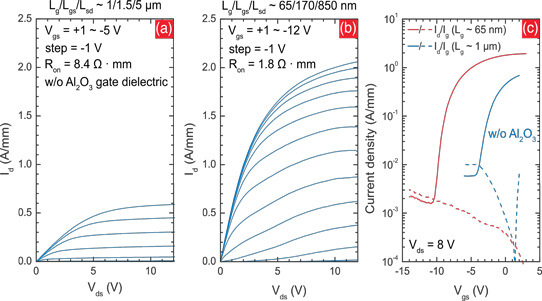
Figure 2: DC common-source family of current-voltage characteristics (I-V) for (a)1μm and (b) 65nm gate AlN/GaN/AlN FETs. (c) Transfer characteristics of both FETs in semi-log scale.
The on-resistance of the long- and short-channel FETs was 8.4Ω-mm and 1.8Ω-mm, respectively. The short-channel device had a high output conductance due to short-channel effects that the researchers believe could be suppressed by using thinner QW and gate barrier stacks. A thinner QW would bring increased benefits from the AlN back barrier.
Studies of the gate leakage indicated that the non-optimal MBE process generated defects. The gate leakage was reduced in the short-channel devices by the Al2O3, improving the on/off current ratio by three orders of magnitude.
The peak extrinsic transconductance of the 65nm FET came in at 250mS/mm, at -6.8V gate potential and 8V drain bias. Correcting for source access resistance, the intrinsic transconductance was 270mS/mm. The threshold voltage was -9.1V, giving normally-on behavior, reflecting the high sheet carrier density and the gate capacitance.
Pulsed large-signal (10V) measurements showed an 18% gate lag and a 16% drain lag. Improved large-signal performance and environmental robustness are expected from the use of passivation to reduce the effects of surface states.
Radio frequency (0.25-30GHz) measurements gave a 120GHz current-gain cut-off (fT) and 24GHz power-gain cut-off (fmax). The low fmax could be improved by moving from rectangular to T-gate structures,
The researchers suggest that using thicker large-bandgap AlN barrier layers with AlGaN channels could achieve improvements in breakdown characteristics and thermal handling over existing state-of-the-art and could lead to high-power applications.
AlN/GaN/AlN quantum well FETs Bulk AlN substrates MBE
http://dx.doi.org/10.1063/1.4975702
The author Mike Cooke is a freelance technology journalist who has worked in the semiconductor and advanced technology sectors since 1997.


