


- News
1 February 2017
Gold-free vertical gallium nitride Schottky barrier diodes
Researchers in China and Japan have developed a gold-free Schottky contact for gallium nitride (GaN), claiming record on/off current ratio and breakdown voltage for vertical GaN Schottky barrier diodes (SBDs) [Xinke Liu et al, Jpn. J. Appl. Phys., vol56, p026501, 2017].
The team from Shenzhen University, Shanghai University, Shanghai Institute of Microsystem and Information Technology, Suzhou Institute of Nano-Tech and Nano-Bionics (SINANO) in China and Tokushima University in Japan believe that such a development could lead to the use of underutilized small-diameter silicon CMOS fabrication facilities. They explain: "In silicon CMOS foundries, gold is typically not used in the front-end process, because gold could cause deep-level traps in silicon, which are the carrier recombination centers that can reduce the carrier lifetime in silicon." Usually, Schottky contacts on GaN use nickel and gold.
Vertical devices are mainly fabricated from material grown on expensive free-standing GaN substrates. However, such devices should make better use of GaN's material properties such as ultralow conduction loss under high voltage and high temperature than the restriction to lateral devices of GaN grown on foreign substrates such as sapphire, silicon carbide or silicon. In addition, free-standing GaN has much lower dislocation densities, which is vital for efficient vertical high-current conduction.
"These devices could be generally useful for cost-competitive power switching circuits with a supply voltage in the range of 500–700V," the researchers write.
The 2-inch free-standing (0001) GaN wafer was grown by hydride vapor phase epitaxy (HVPE) with typical defect density of ~105/cm2. The resistivity was around 0.01Ω-cm and the surface roughness around 0.2nm. A 13μm GaN layer was added by metal-organic chemical vapor deposition (MOCVD). The background doping was around 7x10¹⁵/cm3. Hall mobility was measured at ~1250cm2/V-s.
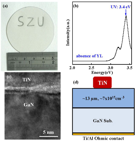
Figure 1: (a) Photograph of FS-GaN wafer. (b) Room-temperature photoluminescence spectrum of FS-GaN wafer with strong peak at 3.4eV from near-band-edge ultraviolet transition. (c) Transmission electron microscope cross-section of TiN/GaN stack. (d) Schematic of fabricated vertical GaN SBDs.
The 250μm-diameter circular SBD structure consisted of 100nm sputtered titanium nitride (TiN) that was etched into an electrode through chlorine-based plasma reactive ion etch (Figure 1). The etch process had a selectivity factor for TiN over GaN of around 100. The back-side contact consisted of alloyed 50nm Ti and 200nm aluminium.
The turn-on voltage of the SBD was around 0.69V. The ideality and Schottky barrier height were 1.1eV and 0.92eV , respectively. The saturation current under reverse bias was 1.8x10⁻¹²A, close to the value of 2.5x10⁻¹²A expected on the basis of forward bias behavior. The on/off current ratio (Ion/Ioff) was 2.3x10¹⁰ using measurements at +1.6V and -2V.
Hard breakdown (VBR) under reverse bias occurred at 1200V. The researchers suggest that the breakdown mechanism could be impact ionization. The power device figure of merit (FOM) VBR2/Ron was 2.1x10⁸V2/Ω-cm2, using the specific on-resistance (Ron) of 7mΩ-cm2 from the linear region of the current-voltage curve. The team plotted benchmark comparisons of Ron, VBR, Ion/Ioff, and FOM (Figure 2).
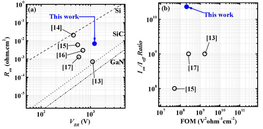
Figure 2: Open symbols: GaN SBDs with gold; solid symbols: GaN SBDs without gold: (a) VBR versus Ron and (b) Ion/Ioff ratio versus FOM of fabricated and state-of-the-art GaN SBDs.
The researchers comment: "Compared with other reported GaN SBDs, the GaN SBDs in this work fabricated with a gold-free process, shows the highest breakdown voltage of 1200V. However, the on-state resistance of the fabricated GaN SBDs in this work is slightly higher, implying that further reduction in non-gold ohmic contact resistance is required."
Schottky barrier diodes GaN HVPE MOCVD
https://doi.org/10.7567/JJAP.56.026501
The author Mike Cooke is a freelance technology journalist who has worked in the semiconductor and advanced technology sectors since 1997.


