


- News
3 February 2017
N-polar gallium nitride gives record power density and efficiency at 94GHz
University of California Santa Barbara (UCSB) in the USA claims record power density (6.7mW/mm) and power-added efficiency (16.9% PAE) at the 'W-band' frequency of 94GHz for metal-insulator-semiconductor high-electron-mobility transistors (MISHEMTs) based on N-polar gallium nitride (GaN) [Steven Wienecke et al, IEEE Electron Device Letters, published online 16 January 2017].
The electric field arising from charge polarization field effects in the N-polar devices is opposite to that in the more usual Ga-polar material used for GaN HEMTs. "For N-polar, the polarization fields create a natural back-barrier that displaces the [two-dimensional electron gas (2DEG)] towards the gate electrode and decouples the design of the primary charge inducing layers and the gate barrier," the researchers explain.
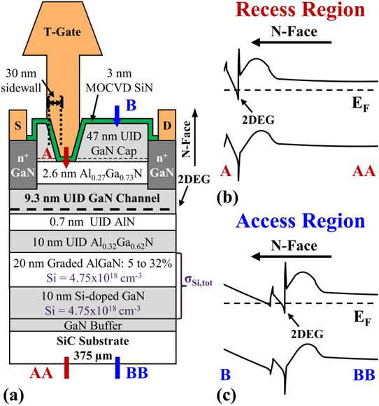
Figure 1: (a) Cross-section of N-polar GaN cap MISHEMT device structure (not to scale). Calculated energy band diagram at equilibrium in (b) gate recess and (c) access regions.
The material was grown by metal-organic chemical vapor deposition (MOCVD) on silicon carbide (Figure 1). The n+-GaN in the source-drain access regions was grown by plasma-assisted molecular beam epitaxy (PAMBE). The access regions were found to have 220Ω/square resistance, compared with 385Ω/square in the gate recess region.
The fabricated devices had 45nm gate-foot length and 2x25μm width. The gate-top length was 450nm. The source-drain distance was 600nm, and the gate-source distance was 125nm. The 375μm silicon carbide (SiC) substrate was not thinned. Measurements were performed on-wafer.
The peak DC extrinsic transconductance was 650mS/mm with 5V drain bias. The maximum drain current (I) at 0V gate potential was 1.9A/mm with 0.61Ω-mm on-resistance. The researchers report: "No current collapse or knee walkout is seen in pulsed IV, illustrating the effectiveness of the N-polar GaN cap design in mitigating dispersion"
Frequency measurements were made up to 67GHz, resulting in cut-off frequencies of 112GHz for current (fT) and 323GHz for power gain (fmax) with the effects of contact pads 'de-embedded'. The quiescent bias conditions were -1.75V gate potential, 13V drain bias, and 1.03A/mm drain current.
The 94GHz power performance was measured using a passive-tuner load-pull system from Maury Microwave Corp. The uncooled continuous-wave operation was under class-AB amplifier conditions. The nominal quiescent source-drain current was 500mA/mm. The relative high current was chosen to maximize power-added efficiency.
At 16V drain and 444mA/mm current, the maximum total output power (Pout) was 25.26dBm (336mW) with associated PAE of 14.4%. The researchers report: "This corresponds to a very high power density of 6.7W/mm which, to the best of our knowledge, represents the highest output power density ever recorded for a GaN device measured at W-band."
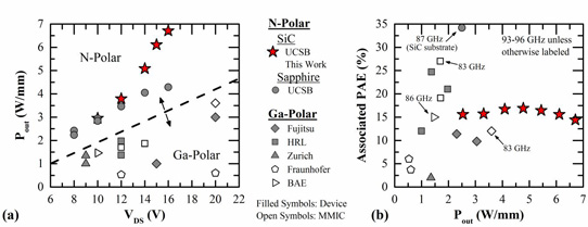
Figure 2: Comparison of W-band (75-110GHz) GaN HEMT technologies at frequencies above 83GHz: (a) output power versus drain bias; (b) associated PAE versus output power. For both plots, open symbols correspond to data taken on monolithic microwave integrated circuits (MMICs) and filled symbols correspond to single device cells either with or without on-wafer pre-matching.
Comparing with other benchmarks (Figure 2), the team adds: "The output power density of this N-polar MISHEMT exceeds that of any reported Ga-polar device by a significant margin and scales extremely well with drain bias, suggesting an RF current swing close to 2A/mm."
The performance does not saturate at higher drain bias. The researchers attribute this to the use of SiC substrates, which has higher thermal conductivity, giving better thermal management and thus reduced self-heating. The maintenance of high PAE at high output power is credited on the N-polar GaN cap removing surface states, and hence dispersion effects (e.g. current collapse), without the use of thick silicon nitride passivation.
The maximum PAE was 16.9%, achieved at 15V drain voltage and 500mA/mm drain current. The associated output power was 4.8mW/mm. By making various improvements, the researchers expect that 22% PAE with no reduction in output power density could be reached using the technology.
The team comments: "A clear pathway towards improved gain and efficiency in load-pull exists through optimization of the existing probe pad layout and a thinning of the SiC substrate. Additional performance enhancements in gain, efficiency and power density are expected with further vertical and lateral scaling of the device dimensions."
They see opportunities for high-power solid-state transmitter applications through greater levels of integration with fewer power-combining stages at both the chip and system level.
GaN MISHEMTs GaN MISHEMTs MOCVD
https://doi.org/10.1109/LED.2017.2653192
The author Mike Cooke is a freelance technology journalist who has worked in the semiconductor and advanced technology sectors since 1997.


