


- News
20 January 2017
Ultra-thin-barrier III-nitride metal-insulator-semiconductor transistors
Researchers in China and Hong Kong have fabricated ultra-thin-barrier (UTB) aluminium gallium nitride (AlGaN) on gallium nitride (GaN) normally-off metal-insulator-semiconductor high-electron-mobility transistors (MIS-HEMTs) with silicon nitride (SiNx) passivation [Sen Huang et al, IEEE Electron Device Letters, vol37, p1617, 2016]. The passivation reduced sheet resistance in the conducting two-dimensional electron gas (2DEG) near the AlGaN/GaN interface by almost an order of magnitude. The structure was grown on low-cost silicon.
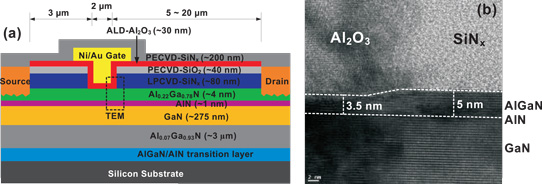
Figure 1: (a) Schematic device structure of normally-off Al2O3/AlGaN/GaN MIS-HEMTs fabricated on UTB AlGaN/GaN heterostructures. (b) TEM cross-sectional view of device's gate corner.
The team from the Institute of Microelectronics of Chinese Academy of Sciences and Suzhou Institute of Nano-Tech and Nano-Bionics in China and Hong Kong University of Science and Technology see potential application in next-generation normally-off power switching devices. Rather than using recess etch of thick AlGaN layers to achieve normally-off behavior, the researchers used a combination of ultra-thin barrier and passivation in the access regions (Figure 1).
The epitaxial material was grown by metal-organic chemical vapor deposition (MOCVD) on 4-inch silicon substrate. The ultra-thin AlGaN barrier on AlN interface enhancement layer resulted in a two-dimensional electron gas (2DEG) with 2.7x10¹²/cm2 carrier density and 2570Ω/square sheet resistance.
Passivation with low-pressure chemical vapor deposition (LPCVD) of 80nm silicon nitride increased the sheet carrier density to 9.5x10¹²/cm2. At the same time, the sheet resistance was reduced to 334Ω/square. The 2DEG mobility was increased to 1980cm2/V-s from the 869cm2/V-s value without passivation. The high mobility is taken as indicating insignificant interface roughness scattering.
The researchers calculated a positive surface charge of 4.56x10¹²/cm2 at the silicon nitride/III-nitride interface from capacitance-voltage measurements. The team further estimates a reduction in the AlGaN surface potential from 1.35eV to 0.49eV. They comment: "The reduction of surface potential of AlGaN barrier by LPCVD-SiNx contributes to an effectively enhanced 2DEG density in UTB AlGaN/GaN heterostructures."
To fabricate devices, the source-drain regions of the silicon nitride were etched using an inductively coupled plasma (ICP) mix of fluorform (CHF3) and sulfur hexafluoride (SF6). The exposed AlGaN was treated with hydrochloric acid. Titanium/aluminium/nickel gold ohmic contacts were deposited and annealed at 830°C in nitrogen.
The gate region was also defined by fluorine-based ICP etch. Aluminium oxide (Al2O3) gate dielectric was applied using atomic layer deposition (ALD). Remote plasma pre-treatment of the Al2O3 deposition surface was used to suppress deep states at the Al2O3/AlGaN interface. The gate electrode was nickel/gold.
The maximum drain current of a MIS-HEMT with 2μm gate length was 661mA/mm at 12V gate potential. The specific on-resistance was 9.0Ω-mm. The gate-drain distance was 10μm. With 1V drain bias, the gate threshold (VTH) for 1μA/mm current was +0.27V. Across a sample of 30 devices, the threshold standard deviation was 0.15V.
The researchers comment: "Owing to the as-grown ultra-thin AlGaN barrier, intentional recess etching of the AlGaN barrier is eliminated, contributing to improved VTH controllability and uniformity."
The vertical breakdown voltage was 695V. Three-terminal breakdown occurred at 1089V, according to a leakage criterion of 1μA/mm with substrate floating. The breakdown path was source to drain. The three-terminal breakdown voltage reduced to 617V with a 5μm gate-to-drain distance.
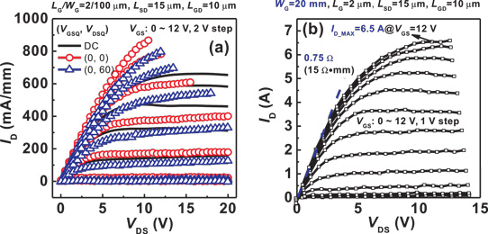
Figure 2: (a) Pulsed drain current (ID) versus drain bias (VDS) characteristics of fabricated normally-off Al2O3/AlGaN/GaN MIS-HEMTs from various quiescent bias points (VGSQ,VDSQ). (b) Characteristics of fabricated 20mm-gate-width devices.
Operation with 200ns pulses at 10μs period increased dynamic on-resistance by 10% (Figure 2), indicating some current collapse. The researchers suggest the increased resistance could be due to oxidation during transfer between AlGaN barrier surface cleaning and growth of the silicon nitride passivation. Alternatively, border/bulk traps could be present in the passivation.
Devices with 20mm gate width achieved normally-off operation with 0.75Ω on-resistance and maximum drain current of 6.5A.
https://doi.org/10.1109/LED.2016.2617381
The author Mike Cooke is a freelance technology journalist who has worked in the semiconductor and advanced technology sectors since 1997.


