


- News
23 January 2017
Interface engineering for green indium gallium nitride laser diodes
University of Chinese Academy of Sciences has developed an interface engineering thermal treatment of indium gallium nitride (InGaN) quantum well active regions in green laser diode (LD) structures [Aiqin Tian et al, Optics Express, vol25, p415, 2017]. The resulting laser diodes had a low threshold current density of 1.85kA/cm2 under continuous-wave operation at room temperature.
Green laser diodes should lead to more compact projectors and other display technologies based on laser light. At present, green light for such applications tends to use non-linear optics to frequency shift light produced at other wavelengths, increasing device sizes and reducing power efficiency.
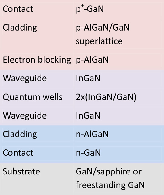
Figure 1: Epitaxial structure.
The green laser diode structures were grown by metal-organic chemical vapor deposition (MOCVD) – see Figure 1. The material quality of the wells was improved by thermal ramping from 700°C to 850°C over 240 seconds and holding for 30 seconds before growing the 15nm GaN barrier at 850°C. The indium layer was protected from loss of indium during the thermal treatment by a 1.8nm GaN cap layer grown at 700°C.
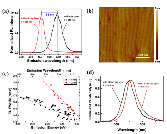
Figure 2: (a) Photoluminescence (PL) spectra of green InGaN/GaN QWs with and without GaN cap layer, (b) atomic force microscope (AFM) images of 15nm quantum barrier layers on GaN/sapphire template, (c) electroluminescence full-width at half maximum (FWHM) dependent on emission energy of laser diode groups with 1.2nm and 1.8nm GaN cap layer, (d) PL spectra of green InGaN/GaN QW with 1.2nm and 1.8nm GaN cap layer.
The thermal treatment suppressed trench defects and removed indium clusters that arise from severe segregation effects usually seen in the high-indium-content InGaN needed for green light emission (Figure 2). The treatment process was developed using material grown on GaN/sapphire templates and free-standing GaN. Electroluminescence and cathodoluminescence studies showed that the indium clusters were formed both at and away from dislocations.
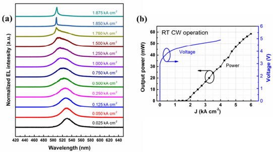
Figure 3: (a) Emission spectra at different current density. (b) Power-current-voltage curve of typical green laser diode under continuous-wave operation at room temperature.
The laser diodes used material deposited on free-standing GaN. Laser diodes with 10µm ridge-waveguide width and 800µm cavity length had a threshold current density of 1.85kA/cm2 under continuous-wave operation at room temperature (Figure 3). A low voltage of 4V at threshold is attributed to suppressed carbon impurity in magnesium-doped AlGaN cladding layer. At 6kA/cm2 injection the output power was 58mW. The green laser wavelength was around 508nm.
Green InGaN laser diodes InGaN MOCVD
http://dx.doi.org/10.1364/OE.25.000415
The author Mike Cooke is a freelance technology journalist who has worked in the semiconductor and advanced technology sectors since 1997.


