


- News
4 January 2017
Understanding graphene-semiconductor Schottky contacts
Researchers in Singapore, the USA and Italy have been developing a modified model of Schottky contacts between graphene (Gr) and two-dimensional (2D) and three-dimensional (3D) semiconductors [Shi-Jun Liang et al, International Electron Devices Meeting, session 14.4, 2016].
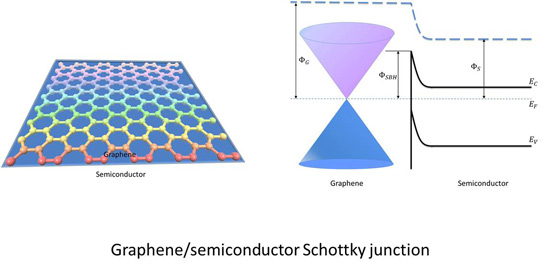
Figure 1: Gr/semiconductor Schottky junction.
The model takes better account of the effective 'zero mass' and zero gap (semi-metal) conduction/valence band structure of Gr with approximately linear energy-wavevector relations (Figure 1). Metals and semiconductors are usually modeled with quadratic energy-wavevector relations, giving non-zero effective mass.
The team from Singapore University of Technology and Design, Lawrence Berkeley National Laboratory in the USA, University of Salerno and CNR-SPIN Salerno in Italy, and the National University of Singapore and Yale-NUS college in Singapore performed both theoretical and experimental work to validate the model.
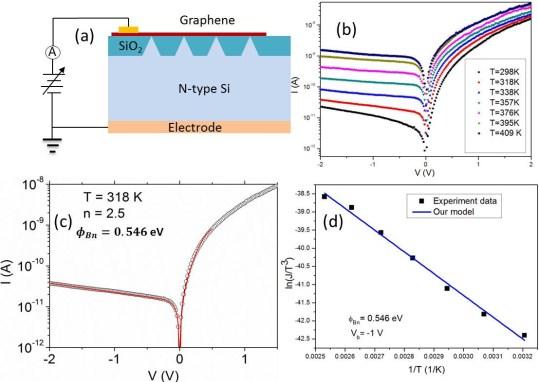
Figure 2: (a) Setup of Gr/n-Si tips Schottky junction device. (b) Current-voltage (I-V) characteristics of device shown in (a) at different temperatures. (c) I-V curve (red solid line) obtained using model with linear dependence of EF on V compared with measured curves (open circle symbol) at 318K. I-V curve at high forward bias is dominated by series resistance and high injection and is not included in fit. (d) Temperature dependence of reverse current at reverse bias of -1V (ln(I/T3) versus 1/T). Extracted reverse current data (square black symbol) compared with model (blue line).
The Gr material was produced by chemical vapor deposition (CVD) on copper. A Gr-silicon junction (Figure 2) was created by placing monolayer Gr on etched nanotips etched on n-type silicon substrates. Measurements were made in the dark at atmospheric pressure.
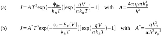
Figure 3: (a) Metal-semiconductor Schottky diode equation. For Gr, mass (m) would be zero, giving zero current density (J). (b) Gr-semiconductor modified Schottky diode equation including effects of ultrafast Fermi velocity (vF) and bias-tunable EF.
The experimental work confirmed the modified Schottky equation (Figure 3) for Gr developed by the team, which describes its modification as "simple and parameter-free". The model also described flat contacts between Gr and silicon, molybdenum diselenide (MoSe2), gallium arsenide (GaAs), and gallium nitride (GaN) (Figure 4).
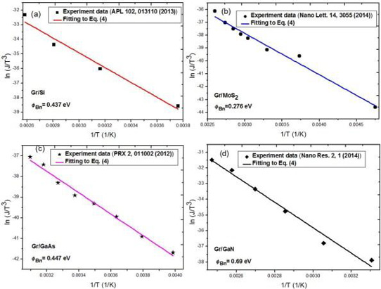
Figure 4: ln(J/T 3 ) versus 1/T for experimental data (symbols) and theoretical results (solid lines): (a) Gr/Si Schottky diode; (b) Gr/MoS2 contact; (c) Gr/GaAs contact; (d) Gr/GaN contact.
The model, based on quantum statistical theory, gave results almost the same as those derived from quantum Landauer transport theory with "excellent agreement", according to the researchers.
The model was also able to take into account Schottky barrier height (φB/ φBn) inhomogeneities that have been found in Gr/Si, Gr/GaAs, and Gr/Ge contacts. The researcher believe the inhomogeneities arise from electron-hole puddles caused by randomly distributed charge impurities. Assuming a Gaussian distribution for the Fermi energy (EF), the Gr/Si, Gr/GaAs and Gr/Ge results were described with standard deviations of 135meV, 98meV and 95meV, respectively.
The researchers found differences in behavior between Gr contacts with two-dimensional (2D, e.g. MoSe2) and three-dimensional (3D, bulk Si, GaAs, GaN, etc.) semiconductors. In the 3D case, the Schottky barrier height was only weakly correlated to the work function. By contrast, strong dependence on work function was found for contacts with 2D semiconductors. The researchers interpret the 2D behavior as showing independence from Fermi pinning effects.
These effects were explained by the team with first-principles calculations.
Graphene semiconductor Schottky contacts Graphene
http://ieee-iedm.org/session-14-modeling-simulation-2d-materials-organic-electronics/
The author Mike Cooke is a freelance technology journalist who has worked in the semiconductor and advanced technology sectors since 1997.


