


- News
9 January 2017
Light transmission from co-integrated laser and modulator on silicon
Researchers in France have co-integrated a 1.3μm III-V laser source with a silicon-based Mach–Zehnder modulator (MZM) [Thomas Ferrotti et al, Optics Express, vol24, p30379, 2016]. Combining semiconductor laser diode technology with silicon photonics would fill the gap for transmitters in the silicon photonics toolbox.
The hybrid III-V/silicon photonics devices were able to transmit information at 25 Gigabits/second at wavelengths of 1303.5nm and 1315.8nm with a 2.5V peak-to-peak signal. The researchers at Université Grenoble Alpes, STMicroelectronics and Université de Lyon see their devices as being compatible with the wavelength-multiplexing requirements of the 100GBASE-LR4 and other communications standards.
Table 1: III-V epitaxy layer structure.
| Layer | Material | Photoluminescence wavelength (μm) | Thickness (nm) | Doping (/cm3 ) |
| p-doped contact | InGaAs | 1.65 | 200 | 2x10¹⁹ |
| Transition | InGaAsP | 1.1 | 50 | 5x10¹⁸ |
| p-doped cladding | InP | 0.92 | 2000 | 2 to 0.5x10¹⁸ |
| SCH | InGaAsP | 1.1 | 100 | Undoped |
| Barriers (x7) | InGaAsP | 1.1 | 10 | Undoped |
| Wells (x8) | InGaAsP | 1.29 | 8 | Undoped |
| SCH | InGaAsP | 1.1 | 100 | Undoped |
| n-doped contact | InP | 0.92 | 110 | 3x10¹⁸ |
| Super-lattice(x2) | InGaAsP | 1.1 | 7.5 | 3x10¹⁸ |
| Super-lattice (x2) | InP | 0.92 | 7.5 | 3x10¹⁸ |
| Bonding interface | InP | 0.92 | 10 | Undoped |
The 1.3μm laser diode active region consisted of indium gallium arsenide phosphide (InGaAsP) multiple quantum wells and barriers surrounded by p- and n-type indium phosphide (InP) – see Table 1. The III-V material for the laser diode measured 700μmx5μmx2.7μm.
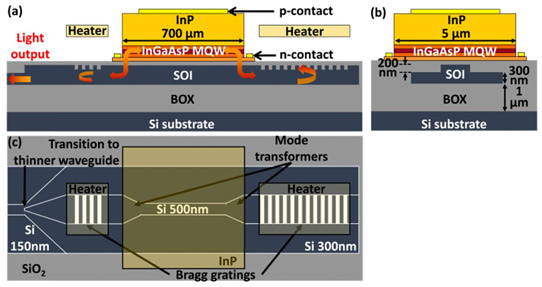
Figure 1: Longitudinal (a), transversal (b) and top (c) schematic views of laser (not to scale!).
The light produced was coupled into the silicon-on-insulator rib waveguide system (Figure 1) through tapered mode transformer regions that led into distributed Bragg reflectors (DBRs) that partially trapped light in a laser cavity. At the back end of the cavity the DBR was highly reflective. The DBR at the laser output end was less reflective, allowing for coupling into the rest of the device.
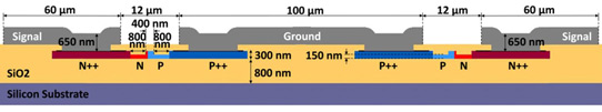
Figure 2: Transversal view of silicon MZM.
Nickel-iron heaters over the DBRs allowed fine tuning of the laser light by increasing the refractive index of the silicon material. The DBR periods provide coarser tuning.
The silicon MZM section used the plasma dispersion effect, where changes in free carrier density alter the real and imaginary parts of the refractive index. The carrier density was controlled by an implanted vertical p-n junction (Figure 2). The effect of hole carriers has more effect than electrons on the real part of the refractive index around 1.3μm.
The modulation was achieved through interference effects between light split and guided down two separate paths, as in Mach–Zehnder interferometry.
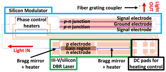
Figure 3: Layout view of complete transmitter integrating hybrid III-V/silicon DBR laser and silicon MZM (2mm-long).
The hybrid laser and MZM were combined (Figure 3) to create a signal transmitter. The phase of the radiation carried by the two arms of the MZM was controlled by a further heater section to give quadrature difference for the selected wavelength.
The structures were produced on 8-inch (200mm) SOI wafers supplied by SOITEC. The oxide layer was 1μm thick. The silicon top layer was 500nm. The handle wafer was high-resistance silicon.
The III-V material was grown on 2-inch (50mm) InP and room-temperature bonded to the SOI wafer. Both surfaces of the bond were activated with oxygen plasma. Post-bond annealing was carried out at 300°C for 2 hours. The InP substrate of the III-V material was removed by hydrochloric acid wet etch.
The SOI/III-V was 'downsized' to 3 inches to allow "processing in a standard III-V platform". The researchers hope to avoid this downsizing in future work.
The laser thresholds were 48mA. The maximum power for single-mode output was up to 52μW with a grating period of 197nm. The MZM length was 2mm, giving an extinction ratio of 2.9dB. With a grating period of 195nm, the threshold was the same, but the maximum output power was 37μW. The 195nm DBR device had a 4mm-long MZM with a larger extinction ratio of 4.7dB.
With currents beyond 100mA and 150mA for the 195nm and 197nm DBR devices, respectively, the emissions became multi-mode. Heating the DBR regions allowed a maximum shift in wavelength of 8.5nm for both devices. The heating efficiency was hampered by a thick layer of silicon nitride between the heaters and the DBRs.
Silicon Mach–Zehnder modulator Laser diodeInGaAsP multiple quantum wells n-type InP
http://dx.doi.org/10.1364/OE.24.030379
The author Mike Cooke is a freelance technology journalist who has worked in the semiconductor and advanced technology sectors since 1997.


