


- News
19 July 2017
High-voltage regrown vertical gallium nitride p-n diodes on bulk substrate
Researchers in USA have been studying regrowth of gallium nitride (GaN) on bulk gallium nitride substrates, claiming the highest breakdown voltage so far for regrown vertical GaN p-n diodes [Zongyang Hu et al, IEEE Electron Device Letters, published online 29 June 2017]. “This is the first high-voltage vertical regrown p-n junction ever reported in the GaN system,” according to the team from Cornell University, University of Notre Dame, and IQE RF LLC, USA.
The power performance is comparable to diodes produced without regrowth (‘as-grown’) on sapphire substrates, the researchers report. They add: “This work serves as an important step towards understanding the conduction mechanism in regrown junctions and improving selective doping technique for high-performance vertical GaN switches.”
Selective doping is needed for current apertures formed from lateral p-n junctions or for embedded p-n junctions in vertical switches.
The n-type part of the device was grown by metal-organic chemical vapor deposition (MOCVD) in the form of an 8μm GaN layer with ~2x10¹⁶/cm3 silicon doping on commercial bulk GaN. The surface was then cleaned with hydrochloric acid before molecular beam epitaxy (MBE) of 400nm ~1018/cm3 magnesium-doped p-GaN and 20nm p++-GaN cap.
MOCVD has problems in regrowth such as high leakage in non-planar structures and strong dependence of impurity incorporation on crystal orientation. There are also problems with forming sharp boundaries between p- and n-type material due to the magnesium memory/diffusion effect. Also, the presence of hydrogen in MOCVD passivates the effectiveness of magnesium doping in creating p-type conduction.
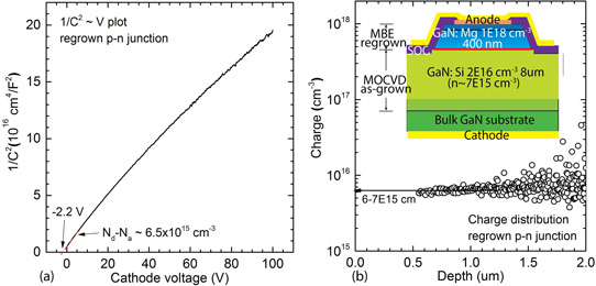
Figure 1: (a) Inverse-square capacitance (1/C2) as a function of reverse voltage measured on regrown GaN p-n diodes and (b) extracted net doping concentration in n-GaN drift layer. Inset: schematic cross-section of completed device.
The fabricated diode was a bevel structure etched down to the n-GaN (Figure 1). The anode was palladium/gold and the cathode titanium/gold. The device was passivated with spin-on glass (SOG). Edge-termination was achieved with an anode field plate that extended outside the mesa edge.
Capacitance-voltage measurements suggested a reduced built-in voltage of the p-n junction (~2.2V), compared with ‘as-grown’ junctions (~3.2V). The researchers tentatively attribute the reduction to band-bending, arising from increased defect density.
The regrown diode further suffers from higher leakage before, and lower output current after, turn-on at more than 3.2V. Reverse-bias leakage in the regrown diode was below the measurement capability of the test equipment for voltages less than 1V, giving an on/off current ratio of 11 orders of magnitude. The ideality factor was greater than 2 at all bias voltages.
The 300-600nm emission from electroluminescence was 30 times lower than for as-grown devices. “This is another direct evidence that the regrown interface contains much more non-radiative recombination centers than the bulk material,” the researchers comment.
The researchers also note that the differential on-resistance (Ron) increased with temperature from 25°C to 125°C. “This trend suggests that the dominant component of Ron in the regrown diode is the n-layer resistance (rn), since electron mobility in the lightly doped n-GaN with low dislocation densities is significantly limited by phonon scattering, thus decreasing with increasing temperature,” they write.
At 800A/cm2 current density, the Ron was ~3.9mΩ-cm2 for regrown diodes and ~0.6mΩ-cm2 for as-grown.
The maximum reverse-bias breakdown of the regrown diodes was 1136V for a 107μm-diameter device. The leakage before breakdown was 0.1A/cm2. “Most breakdown events were destructive and no avalanche breakdown behavior could be measured, unlike in the as-grown p-n diodes,” the team reports.
Study of the current-voltage behavior suggests that Frenkel-Poole field-assisted thermionic emission was the dominant leakage mechanism below 160V reverse bias. This changed to variable range hopping in the depletion region as breakdown approached, it is thought.
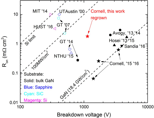
Figure 2: On-resistance versus breakdown voltage benchmark plot of state-of-the-art high-voltage GaN p-n diodes on GaN, SiC, sapphire and silicon substrates.
Comparing the breakdown voltage (BV) and 800A/cm2 Ron (Figure 2) through the ratio BV2/Ron gives 0.33GW/cm2 for the regrown diode and 4.1GW/cm2 for the as-grown device.
GaN p-n diodes GaN MOCVD Sapphire substrates
https://doi.org/10.1109/LED.2017.2720747
The author Mike Cooke is a freelance technology journalist who has worked in the semiconductor and advanced technology sectors since 1997.


