


- News
15 June 2017
Imec achieves record-low source/drain contact resistivity for PMOS transistors
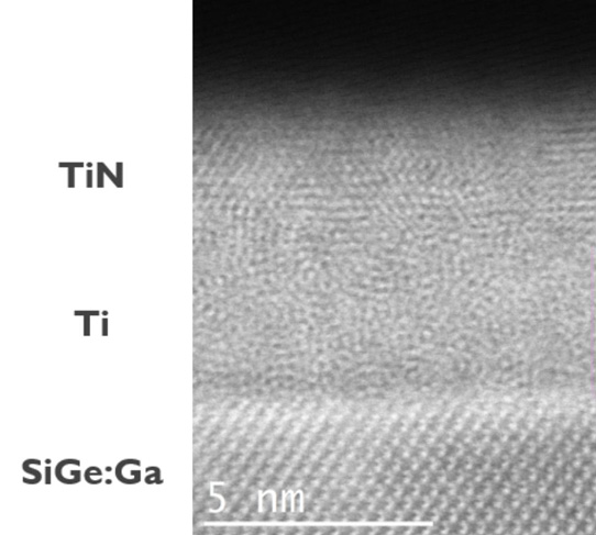
At the 2017 Symposia on VLSI Technology and Circuits in Kyoto, Japan (5-8 June), nanoelectronics and photovoltaics research centre Imec of Leuven, Belgium reported record values below 10-9Ω.cm2 for PMOS source/drain contact resistivity. Results were obtained through shallow gallium implantation on p-type silicon-germanium (p-SiGe) source/drain contacts with subsequent pulsed nanosecond laser anneal.
In future N7/N5 nodes, the source/drain contact area of the transistors becomes so small that the contact resistance threatens to become the dominating parasitic factor, resulting in suboptimal transistor functioning. Researchers have therefore been working on techniques to reduce the contact resistance on highly doped n-Si and p-SiGe source/drain contacts, aiming for values below 10-9Ω.cm2. Together with colleagues from the Katholieke Universiteit Leuven (KU Leuven) in Belgium, Fudan University in Shanghai, China, and Applied Materials in Sunnyvale, CA, USA, Imec concentrated on p-SiGe contacts, comparing the effects of high-dose boron and gallium doping.
For comparison, the researchers implanted SiGe separate wafers with a high dose of gallium or boron and applied various anneal processes. They then fabricated multi-ring circular transmission line model (TLM) structures, which are highly sensitive to contact resistance. Subsequent measurements revealed the lowest contact resistance for the gallium-implanted structures annealed with Applied Material’s nanosecond laser anneal. This process uniquely causes a Ge/Ga surface segregation, which is responsible for the ultralow sub-10-9Ω.cm2 contact resistivity. This result shows a possible way to process next-generation technology nodes.
“This breakthrough achievement in our search to develop solutions for next-generation deeply scaled CMOS provides a possible path for further performance improvement using the current source/drain schemes in N7/N5 nodes,” says Naoto Horiguchi, distinguished member of the technical staff at Imec.
Imec’s research into advanced logic scaling is performed in cooperation with key partners in its core CMOS programs including GlobalFoundries, Huawei, Intel, Micron, Qualcomm, Samsung, SK Hynix, Sony Semiconductor Solutions and TSMC.


