


- News
28 June 2017
Indium tin oxide metal-organic chemical vapor deposition for UV LEDs
Sun Yat-Sen University in China has been developing a metal-organic chemical vapor deposition (MOCVD) indium tin oxide (ITO) process with a view to creating ultraviolet transparent conductive electrodes for aluminium gallium nitride (AlGaN) light-emitting diodes (LEDs) [Zimin Chen et al, Appl. Phys. Lett., vol110, p242101, 2017].
Although ITO is one among many possibilities for visible light transparent conductive layers, these materials, including ITO, tend to become less transparent at shorter ultraviolet wavelengths. The Sun Yat-Sen team has managed to widen the optical bandgap to 4.7eV through MOCVD growth. A photon of 4.7eV has an ultraviolet wavelength of 364nm.
Ultraviolet semiconductor devices are being developed with a view to water purification, biological detection, medical diagnostics, UV curing and other applications.
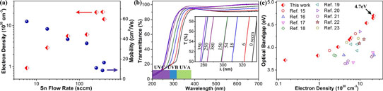
Figure 1: Electrical and optical properties of 90nm-thick MOCVD-ITOs. (a) Dependence of electron density and mobility on Sn flow rate. (b) UV-visible transmittance of MOCVD-ITO with different Sn flow rates. Inset: blue-shift of absorption edge. (c) Comparison of optical bandgap of ITO grown by different techniques.
The Sun Yat-Sen researchers first used MOCVD to grow 90nm ITO layers on sapphire at ~500°C (Figure 1). The precursors were trimethyl indium (TMIn), tetrakis-dimethylamino tin (TDMASn), and oxygen carried in argon. The resulting material was textured with pyramid-like shape (100) and triangle or truncated-triangle plate-like shape (111) grains.
The increase of tin content to 350 standard cubic centimeters per minute of precursor resulted in the highest free electron density (2.15x10²¹/cm3) and an increase in the optical bandgap to 4.70eV. The free electron density in indium oxide (In2O3, zero TDMASn precursor) was 1.47x10¹⁹/cm3, giving a bandgap of 3.72eV. The impact of free electrons on the bandgap was attributed to the Burstein-Moss effect, where electrons fill the lower conduction band states and hence increase the photon energy needed to excite electrons from the valence band. “The widening of bandgap as large as ΔEg = 0.98eV is rarely reported to date,” the team comments.
The team also believes MOCVD avoids lattice distortion by improving crystal quality. Lattice distortion can be a factor that narrows optical bandgaps in ITO.
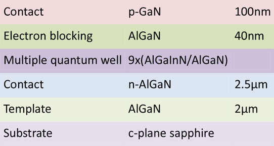
Figure 2: Epitaxial structure of LED.
UV LEDs were also produced using MOCVD (Figure 2). Magneto-sputtering ITO was compared with MOCVD-ITO for use as a 120nm-thick transparent conducting p-electrode. The target tin/indium oxide (SnO2:In2O3) ratio was 1:9 by weight. The magneto-sputtered material was annealed at 550°C for 5 minutes in nitrogen. The ITO thickness was designed to improve current spreading. The 1143μmx1143μm LEDs were completed with chromium/palladium/gold contact pads.
The LED wavelength was 368nm. At this wavelength, the sputtered-ITO had 86% transmittance, while the MOCVD-ITO managed 95%. While the resistivity of the sputtered-ITO was less than that of the MOCVD-ITO, the sputtered contact resistance was greater.
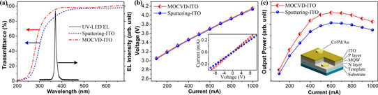
Figure 3: (a) Transmittance of 120nm-thick MOCVD-ITO and sputtering-ITO grown on sapphire. Electroluminescence spectrum of LEDs with MOCVD-ITO electrodes is also shown. (b) Voltage-current (V-I) characteristics of LEDs. Inset: I-V characteristics of ITO/LED contact. (c) Output power versus current characteristics. Inset: LED schematic.
The result of using MOCVD-ITO was an increase in output power of 11.4% at 350mA and 14.8% under 600mA injection (Figure 3). The 350mA operating voltage was 3.45V, averaged over 2000 devices. The voltage-current behavior of the two devices was basically the same over the operating range.
Indium tin oxide MOCVD UV LEDs AlGaN
http://dx.doi.org/10.1063/1.4986452
The author Mike Cooke is a freelance technology journalist who has worked in the semiconductor and advanced technology sectors since 1997.


