


- News
20 June 2017
Gallium nitride implanted current-aperture vertical electron transistor
University of California Davis (UC Davis) and University of California Santa Barbara (UCSB) in the USA have claimed the first demonstration of an implantation-based current-aperture vertical electron transistor (CAVET), grown on sapphire, blocking 450V with respectable on-state characteristics [Saptarshi Mandal et al, IEEE Electron Device Letters, published online 30 May 2017].
Vertical devices are probably needed for higher power handling beyond 15kW, while the more widely developed lateral power devices seem to be economical up to 10kW.
The CAVET (Figure 1) 1μm n+-GaN drain, 6μm n--GaN drift and 300nm lightly doped n-GaN aperture layers were grown by metal-organic chemical vapor deposition (MOCVD). The current-blocking layer (CBL) aperture was defined by magnesium ion implantation with a photoresist mask. The aperture area (AAP) was 394μm2 and the CBL area (ACBL) was 2490μm2. The ion implant energy was varied to give a box profile.
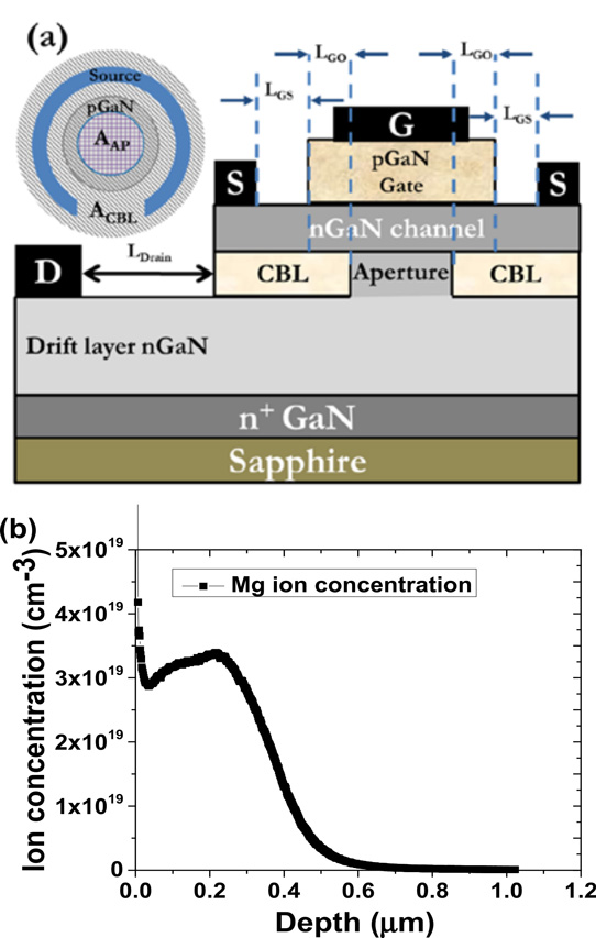
Figure 1: (a) Device structure of CAVET. Inset: top-view. The inner shaded area is the aperture and the outer shaded area is the CBL; p-GaN covers the entire aperture area. (b) Magnesium (Mg) ion distribution of implanted profile, as obtained from secondary-ion mass-spectrometry (SIMS).
The channel region was grown using ammonia-based molecular beam epitaxy (MBE). The advantage of this is a lower growth temperature, which reduces loss of magnesium doping through out-diffusion from the CBL into the channel layer.
The channel consisted of 15nm carbon-doped GaN and 300nm silicon-doped n-GaN. The aim of the carbon-doping was to compensate for a silicon excess on the growth surface which could not be removed by photoresist cleaning processes involving hydrogen fluoride, oxygen plasma clean and heated n-methyl-2- pyrrolidone.
The material structure was completed with 100nm of p-GaN, which became the gate insulator in the CAVET. The p-GaN gate-aperture overlap (LGO) was 5μm. Such p-GaN gates are expected to have reduced leakage compared with the AlGaN/GaN Schottky barrier often used in lateral devices.
The CAVET fabrication used inductively coupled etching of the access regions. Electrical isolation was achieved through forming 1μm deep mesas.
The drain consisted of an etched 1μm-deep 2.4mm-diameter circle. The source and drain contact metals were titanium/aluminium/nickel/gold. The metal stack was annealed at low temperature (735°C) to avoid the source metals spiking into the CBL. The p-GaN-source distance (LGS) was 4μm. The drain contact to device distance (LDrain) was 20mm.
The gate metal stack was palladium/nickel/gold. A 500nm layer of plasma-enhance chemical vapor deposition (PECVD) silicon nitride was used as passivation.
The maximum drain current density was 600A/cm2 with 30V drain bias and +4V gate potential. The density was relative to the area enclosed by the source electrode. The device pinched off at -10V gate potential with 30V drain bias.
Pulsed operation saw no reduced current (‘collapse’) or dispersion from the static DC results. The researchers attribute this to the CAVET structure with the high-electric-field region buried in the drift region, away from the surface, unlike in lateral devices such as high-electron-mobility transistors (HEMTs). In fact, the researchers add: “The DC characteristics showed a reduction in current, which could be attributed to self-heating effects due to longer bias times.” Sapphire is thermally insulating, reducing heat dissipation.
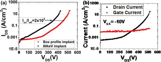
Figure 2: (a) Three-terminal breakdown of CAVET with box profile and single-energy (80keV) implanted CBL. (b) Gate and drain leakage current during breakdown measurement.
The three-terminal breakdown in the pinch-off state was estimated at 450V for 1mA maximum current, and on/off current ratio of 2x10³ (Figure 2). In fact, the devices were able to withstand 520V. The researchers comment: “This is the highest reported breakdown for CAVETs with implanted CBL. The off-state leakage at a given voltage is also two orders of magnitude lower than existing state-of-art AlGaN/GaN CAVETs with ion-implanted CBL.”
The source-gate leakage was initially higher than the source-drain leakage. However, at 350V drain bias the source-drain leakage begins to dominate up until breakdown. The gate-source leakage was tentatively attributed to current flow along the etched p-GaN sidewall. The drain-source leakage was attributed to breakdown/shorting of the CBL.
UCSB GaN Current-aperture vertical electron transistor PECVD
https://doi.org/10.1109/LED.2017.2709940
The author Mike Cooke is a freelance technology journalist who has worked in the semiconductor and advanced technology sectors since 1997.


