


- News
30 March 2017
Non-polar gallium nitride ultraviolet photodetector on sapphire
CSIR-National Physical Laboratory (CSIR-NPL) in India has used non-polar (NP) a-plane (11-20) gallium nitride (GaN) on r-plane (1-102) sapphire to create an ultraviolet (UV) photodetector with improved performance over previous devices using the same crystal structures [Abhiram Gundimeda et al, Appl. Phys. Lett., vol110, p103507, 2017]. In particular, the responsivity of 340mA/W at 5V bias is the best performance reported for a-GaN/r-sapphire films, the team claims.
The researchers see the high thermal stability, high radiation resistance and other properties of GaN as offering high-gain and high-speed UV photodetection for applications such as space communications, flame sensors, atmospheric ozone detection, biophotonics, and electromagnetic polarization-sensitive detection.
Normally GaN is grown in the polar c-plane orientation, where the charge polarization of the chemical bonds leads to strain-dependent and spontaneous electric fields that hamper device performance. Other orientations such as a-plane often involves growth on free-standing or bulk GaN substrates, which are much more expensive than c-plane sapphire. A-plane material can result from growth on r-plane sapphire, but the resulting epitaxial GaN usually has poor quality.
Plasma-assisted molecular beam epitaxy (PAMBE) was used to grow non-polar a-plane GaN on r-plane sapphire substrate. Growth began with 490°C nitridation and low-temperature 530°C GaN buffer. Further PAMBE at 745°C gave a 631nm GaN layer. The atomic composition was 51% gallium and 49% nitrogen, according to Rutherford back-scattering analysis.
X-ray analysis suggested that the material was nearly stress-free. The threading dislocation density was estimated to be 8x10⁹/cm2 on the basis of x-ray rocking curve peak widths. The researchers claim that the material had the lowest dislocation density and narrowest peak width compared with non-polar GaN grown on r-plane sapphire by other techniques. These other techniques tend to give threading dislocation densities of 1010/cm2 and greater.
Photoluminescence gave a narrow near-band-edge peak at 3.39eV, a 10meV red-shift from strain-free GaN (3.40eV). There were also low-intensity broad peaks in the yellow (~2.2eV) and blue (~3.0eV) bands. Yellow emission is often associated with defects. The blue luminescence is attributed to dissociation of excitons (electron-hole pairs) bounded to neutral donors.
The researchers comment: “The strong, narrow band-edge emission along with low intense defect bands exhibits that the GaN layer has a superior optical quality (implies a low density of native defects).”
The surface of the GaN layer had two-faceted triangular island structures, which resulted in the low stress, according to Raman analysis.
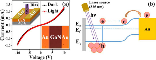
Figure 1: (a) Current-voltage curve of GaN PD under dark and light conditions. Inset: schematic diagram and optical image of fabricated UV PD. (b) Energy-level diagram of Au/GaN junction showing charge transfer under UV illumination.
UV photodiodes were fabricated by depositing and patterning 150nm-thick gold contacts separated by 60μm to give a metal-semiconductor-metal geometry. With 5V bias, the dark current was 1.5μA (Figure 1). The relatively large dark current “suggests the presence of electrical leakage, which may be associated with extended defects in the epitaxial layers (most likely basal plane stacking faults in NP nitride films),” say the researchers. The difference with the current under 325nm laser illumination was very small. The team suggests that tunneling through defect states may be to blame.
Switching the laser on and off at 10 second intervals gave increased response (Figure 2). The on-current was 2.53μA and 74.49μA with 50mV and 5V bias, respectively. The light power density was 13mW/cm2 and the measurements were at room temperature. The response for 5V bias was 340mA/W.
The researchers comment: “Such a significant enhancement in the photocurrent can be attributed to the dominance of charge generation over charge recombination, thereby producing more charge carriers with increasing bias. Also, the higher bias voltage will enhance the collection of the photo-excited carriers which leads to increased photocurrent.”
The noise equivalent power (NEP) at 5V bias was 2.4x10⁻¹¹W/√Hz, less than for silicon photodiodes. The corresponding specific detectivity figure of merit was 1.24x10⁹Jones. The specific detectivity is inversely proportion to NEP, while normalizing for the effects of device area and frequency bandwidth. A higher detectivity of 1.42x10⁹Jones was achieved at 3V bias.
The researchers comment: “These obtained values of responsivity and detectivity are the highest reported values than any other UV PD device fabricated using epitaxial NP GaN films on sapphire substrate and are comparable with UV PD made of other materials such as oxides and SiC, etc.”
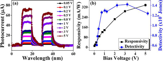
Figure 2: (a) Time-dependent photo-response of GaN UV PD with varying bias under 325nm illumination and (b) variation in responsivity and detectivity with respect to bias voltage.
Finally, the team report on the rise and fall times at 5V bias – 280ms and 450ms, respectively. The longer fall time is attributed to delays in decay of photo-generated carrier density. They comment: “In comparison with previous reports, which show response times in seconds, our detectors are producing response times in the order of milliseconds. Such a high-speed and enhanced photo-response is conceivable due to low-trap-density, high-crystalline GaN film.”
GaN Sapphire UV photodetector PAMBE
http://dx.doi.org/10.1063/1.4978427
The author Mike Cooke is a freelance technology journalist who has worked in the semiconductor and advanced technology sectors since 1997.


