


- News
15 March 2017
Imec’s 200mm GaN-on-Si e-mode power devices withstand heavy ion and neutron irradiation
Nanoelectronics and photovoltaics research centre imec of Leuven, Belgium says that – in tests performed in collaboration with Thales Alenia Space Belgium (the country’s largest manufacturer of space electronics) – its 200mm gallium nitride-on-silicon (GaN-on-Si) enhancement-mode (E-mode) power devices with a p-GaN gate architecture have shown no degradation after heavy ion and neutron irradiation, demonstrating that its 200mm GaN-on-Si platform delivers GaN-based power devices for earth as well as for space applications.
Since GaN-on-Si transistors operate at higher voltages, frequencies and temperatures than their silicon counterparts, they are ideal candidates for power conversion devices as they show less power losses in electricity conversion. First-generation GaN-based power devices are used currently and will play a key role in the power conversion of future electronic devices such as battery chargers, smartphones, computers, servers, automotive, lighting systems and photovoltaics.
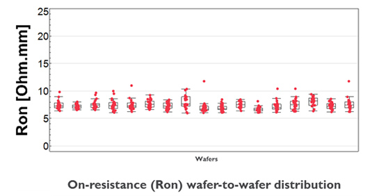
Imec has been developing the next-generation of GaN-based power devices with improved performance and reliability. It says that its latest 200mm GaN-on-Si platform (currently available for dedicated development or technology transfer to imec’s current and future partners) shows good wafer-to-wafer reproducibility and low dynamic Rdson.
Imec’s latest generation of 200mm GaN-on-Si e-mode p-GaN devices were irradiated with heavy ions (xenon) and neutrons. Pre- and post-irradiation tests revealed that there was no permanent degradation of transistor characteristics: neither shifts in threshold voltage nor gate rupture. Radiation hardness of the devices is important, as it enables applications in space, where fluxes of heavy ions and neutrons can damage electronic circuits in satellites and space stations. Wide-bandgap devices promise a significant increase in performance, but robustness to space radiation is essential. The result obtained with Imec’s GaN-on-Si devices is a key step on the path to space-based power conversion applications, it is reckoned.
“It demonstrates that our 200mm GaN-on-Si platform has reached a high level of technology readiness and can be adopted by industry,” believes executive VP Rudi Cartuyvels. “At imec, we use 200mm silicon substrates for GaN epitaxy and this technology can be used on 200mm CMOS-compatible infrastructure,” he adds. “Thanks to innovations in transistor architecture and substrate technology, we’ve succeeded in making GaN devices on larger wafer diameters than used today, which brings lower-cost perspectives for the second generation of GaN-on-Si power devices. Imec is also looking beyond today’s technology, exploring novel substrates, higher levels of integration and novel devices.”
The results were achieved in the framework of the European Space Agency (ESA) project ‘ESA AO/1-7688/13/NL/RA: GaN devices for space based DC-DC power conversion applications’. “GaN is a critical technology for future space missions with a wide range of potential applications, including smaller-size, higher-efficiency DC-DC power conversion subsystems,” says ESA technical officer overseeing the project.
Obtained from the first phase of an ESA GSTP project, the results show that the p-GaN devices developed by imec offer excellent radiation robustness for operation in space. In the second phase of the project it is planned to industrialize this technology in readiness for a future space qualification program”.


