


- News
22 March 2017
Gallium nitride vertical junction barrier Schottky diodes
Cornell University, Qorvo Inc and IQE RF LLC in the USA have reported on work on vertical junction barrier Schottky diodes (JBSDs) produced on free-standing gallium nitride (GaN) [Wenshen Li, et al, IEEE Transactions on Electron Devices, published online 21 February 2017]. The aim was to combine the good characteristics of Schottky barrier diodes and pn diodes (PNDs) for power applications.
SBDs have low turn-on voltage, but suffer from higher current leakage under reverse bias. By contrast, PNDs have high turn-on and low reverse-bias leakage. High current under reverse bias reduces the effective breakdown voltage (BV) characteristics of SBDs.
By using pn and Schottky barrier structures, the JBSD can combine low turn-on with low reverse-bias leakage through reducing the surface field (RESURF). However, attempts to use lateral pn junctions suffer from increased process complexity from using ion implant or re-growth steps.
Instead, Cornell/Qorvo/IQE used a vertical structure with trenches in p-GaN material reaching down to give Schottky contacts with n-GaN (Figure 1).
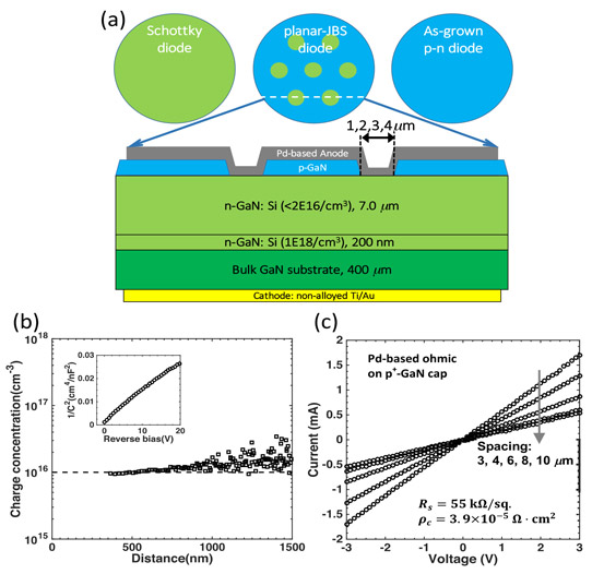
Figure 1: (a) Schematic device top view and cross section of fabricated trench JBSD. Total Schottky (trench) area is designed to be same for each trench diameter. (b) Carrier concentration in n-GaN drift layer extracted by capacitance-voltage measurement at 1MHz. (c) Representative transmission line method current-voltage characteristics of Pd-based ohmic contact on p-GaN with calculated sheet resistance (Rs) and specific contact resistivity (ρc).
The team comments that Panasonic used a similar trench JBSD to give superior breakdown and simultaneously low on-resistance in work presented in 2015. Cornell/Qorvo/IQE add: “However, the RESURF effect could not be explicitly confirmed, since the characteristic shift of the turn-on voltage was not observed and the leakage behavior of the diodes was not reported.”
Metal-organic chemical vapor deposition (MOCVD) on free-standing GaN was used to create the semiconductor material of the diodes. The substrate had a threading dislocation density of ~2x10⁶/cm2. High dislocation densities lead to higher reverse-bias leakage in general. Non-free-standing GaN substrates such as sapphire and silicon carbide tend to lead to higher-dislocation-density GaN epitaxial material due to lattice mismatch.
The trenches for the JBSD structure were formed by dry etching. Circular trenches were chosen since the researchers expected this to result in a more uniform field profile along the periphery, giving a less restricting size constraint compared with striped/linear trenches.
The anode of the diode was palladium (Pd)-based, giving ohmic and Schottky contacts with p-GaN and n-GaN, respectively. The devices were 100μm in diameter. The researchers comment: “No additional field plate (FP) structures are used for edge termination, since the additional leakage often associated with the FP process might mask the trend in the leakage current of trench JBSDs designed with varied trench sizes.”
Simulations with stripe trenches suggested that the surface electric field arising from positive charge under the Schottky contact terminates at the depletion region in the p-GaN instead of the Schottky contact, reducing the surface field’s vertical component.
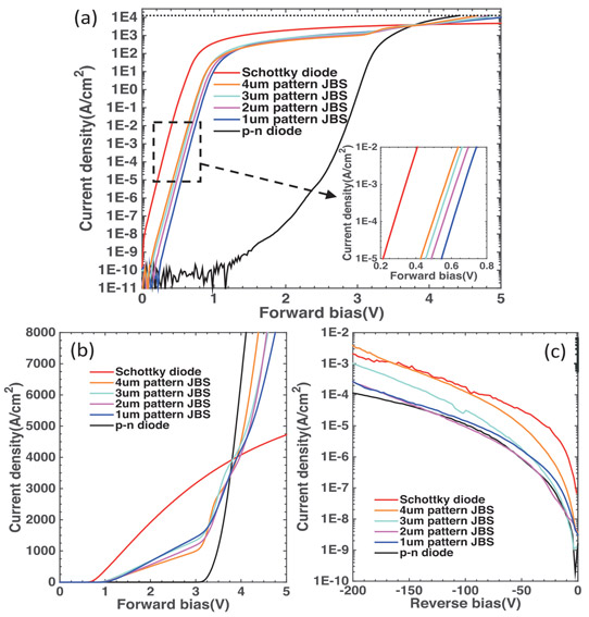
Figure 2: Measured current-voltage characteristics of trench JBSDs. (a) Forward-bias characteristics in log scale. (b) Forward bias in linear scale showing two-step turn-on. (c) Reverse bias in log scale.
The JBSDs and the comparison SBD turned on with around 1V forward bias and ideality factor in the range 1-1.05 (Figure 2). The turn on shifts upwards as the trench becomes smaller. Reverse-bias leakage was reduced as the trench size was scaled downwards. “Up to 20 times reduction in leakage current is achieved in the 1μm trench JBSDs compared with conventional SBDs, reaching the PND leakage level,” the team reports, adding: “As the total trench area is designed to have the same total area, the reduction in leakage current is due to the RESURF effect arising from the trench JBSD design.”
The breakdown voltages of the PND and JBSDs were similar, in the range 250-650V. The SBD breakdown was generally somewhat lower, in the range 275-425V. The SBD performance was probably affected by severe edge field crowding at the anode metal edge. The researchers expect high breakdown voltages with suitable edge termination structures.
The reverse current leakage at 150V bias increased from pure PND to SBD, through increasing trench-size JBSDs. The PND current density leakage was in the range 10-5-10-4A/cm2, while the SBD leakage was spread between ~3x10⁻⁴A/cm2 up to ~10-1A/cm2.
Free-standing GaN GaN JBSDs Cornell University Qorvo IQE Schottky diodes MOCVD
https://doi.org/10.1109/TED.2017.2662702
The author Mike Cooke is a freelance technology journalist who has worked in the semiconductor and advanced technology sectors since 1997.


