


- News
24 March 2017
Semi-polar indium gallium nitride laser diode/waveguide photodiode combo
Researchers based in Saudi Arabia and USA have integrated a waveguide photodetector (WPD) with a 405nm laser diode (LD) using free-standing semi-polar gallium nitride (GaN) technology [Chao Shen et al, Appl. Phys. Express vol10, p042201, 2017]. The semi-polar material reduces electric fields in aluminium indium gallium nitride (AlInGaN) heterostructures that arise from differences in charge polarization of the chemical bonds between the elements. Reducing these fields avoids the detuning between InGaN multiple quantum wells (MQW) laser diode emission and photodetector absorption spectra seen with polar c-plane heterostructures.
The team from King Abdullah University of Science and Technology (KAUST) in Saudi Arabia, University of California Santa Barbara (UCSB) in the USA, and King Abdulaziz City for Science and Technology (KACST) in Saudi Arabia see the integrated device as leading to on-chip power monitoring, visible light communication (VLC), and the implementation of III-nitrides as a photonics platform. Using laser diodes, rather than light-emitting diodes (LEDs), gives benefits in terms of efficiency droop and modulation bandwidth for solid-state lighting and VLC applications.
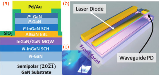
Figure 1: (a) Epitaxial layer structure, (b) schematic of InGaN/GaN MQW based WPD-LD, and (c) photo of laser emission from front facet of WPD-LD.
The epitaxial structure (Figure 1) was grown on (20-2-1) GaN by metal-organic chemical vapor deposition (MOCVD). The MQW structure was four periods of 3.6nm/7nm In0.1Ga0.9N/GaN wells/barriers. The electron-blocking layer (EBL) was 18nm p-type aluminium gallium nitride (p-Al0.18Ga0.82N). The separate-confinement heterostructures (SCHs) were 120nm p/n-InGaN. The cladding layers were 600nm p-GaN and 350nm n-GaN. The contact layers were heavily doped p- and n-type to give ohmic contacts with the palladium/gold and titanium/aluminium/nickel/gold respective contact metallization.
The material was structured into a 505μm-long laser diode with a 90μm-long WPD at its rear facet. The device separation was 5μm. The etched ridge waveguide was 2μm wide. An isolation trench was fabricated by focused ion-beam milling. The facets were uncoated. The electrical isolation of the devices was around 1MΩ, “more than five orders of magnitude higher than the junction series resistance, enabling the independent operation of the two components,” according to the researchers.
The laser diode had a 130mA threshold and 0.4W/A slope efficiency, as determined by a standard calibrated silicon photodetector, with continuous wave (CW) operation at room temperature. The output from the WPD at zero bias followed the performance of the laser diode closely, allowing its use as an on-chip power monitor.
Reverse biasing the WPD resulted in increased response by increasing the depletion region where photons were absorbed, generating a photocurrent. Tests were carried out with pulsed currents on the laser diode to avoid self-heating. At 200mA injection, the laser diode produced WPD currents of 63.5μA, 80.7μA, 112.3μA and 130.4μA under respective reverse biases of 0V, 2V, 4V and 6V. The photocurrent/optical input power responsivity of the WPD increased from 0.018A/W to 0.051A/W as the reverse bias increased from 0V to 10V.
The researchers comment: “Considering the fact that the WPD and LD share the same active layer design without the need of epitaxial re-growth, the presented WPD outperforms other PDs utilizing InGaN/GaN QWs on c-plane-orientated substrates (0.001–0.01A/W at 450nm) for simultaneous light emission and detection. The high responsivity of the WPD is attributed to the enhanced overlap between the absorption peak of the WPD and the emission peak of the LD. The enhancement in the overlap originates from a reduced polarization field in QWs grown on a semi-polar GaN substrate.”
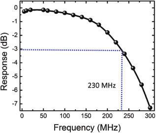 Figure 2: Modulation response of WPD at zero bias.
The frequency response of the system with unbiased WPD was also measured (Figure 2). The 3dB bandwidth was 230MHz. The researchers attribute the bandwidth to the WPD, since laser diode bandwidth was known to be above 1GHz. Despite this, the WPD bandwidth improves on values reported for GaN Schottky barrier PDs (5.4 MHz) and GaN p–i–n PDs (10–20 MHz).
The team comments: “The increased cutoff frequency of the WPD is associated with the reduced device size owing to the narrow ridge design and the improved responsivity of the semi-polar plane WPDs. The high-speed WPD suggests its potential as an integrated receiver for on-chip communication and VLC applications.”
Waveguide photodetector Laser diode Free-standing semi-polar GaN MOCVD
https://doi.org/10.7567/APEX.10.042201
The author Mike Cooke is a freelance technology journalist who has worked in the semiconductor and advanced technology sectors since 1997.


