


- News
2 March 2017
Improving indium arsenide antimonide nanowire optical quality on silicon
Researchers from UK and China have used optimized droplet-assisted molecular beam epitaxy (MBE) to improve the optical quality of indium arsenide antimonide (InAsSb) nanowires (NWs) on silicon with up to 19% Sb content [Q D Zhuang et al, Nanotechnology, vol28, p105710, 2017]. The peak wavelength of the resulting NWs ranged from 3.0μm to 5.1μm.
The 5.1μm wavelength represents the longest to date for InAsSb NWs, according to the team from Lancaster University (UK), Shanghai Institute of Technical Physics (China), University of Warwick (UK), Jianghan University (China), University of Liverpool (UK) and Sun Yat-Sen University (China).
The team believes that the NWs could enable highly efficient silicon-based mid-wave infrared (MWIR, 3-5μm) and even long-wave infrared (LWIR, 8-12μm) photodetectors, operating at room temperature, along with infrared-emitting devices, highly sensitive phototransistors, and renewable electricity generators. They see InAsSb NWs as “an ideal and versatile candidate for a variety of device applications, for instance, in optoelectronics in the infrared and terahertz spectral ranges, high-speed electronics, thermophotovoltaic and thermoelectric devices, and cost-effective biosensors.”
As usual, realizing the possibilities requires improved material. The researchers used a technique where the deposition of indium (In) droplets under pre-optimized conditions nucleates NW growth, avoiding the use of catalysts such as gold or nickel. Antimony has a strong surfactant effect that creates problems for incorporation into InAsSb.
The samples were grown on (111) Si with the composition mainly determined by flux ratios. The researchers found that reducing the V/III ratio favored a higher growth rate of NWs and enhanced Sb incorporation. The researchers comment: “We believe that a faster growth rate reduces the Sb surfactant effect. Meanwhile, the higher growth rate favors Sb incorporation, which is the same as that observed in the epitaxy of InAsSb thin film.”
Table 1: Sb content determined through energy-dispersive x-ray analysis and corresponding theoretical bandgap energy for series of InAsSb NWs with 10K band-to-band photoluminescence peaks and full-width at half maximum (FWHM). Estimated uncertainties for peak and FWHM energies 1.0meV and 1.4meV, respectively.
| Measured Sb content and variation (atm.%) | Peak energy (eV) | FWHM (meV) | Theoretical bandgap (eV) |
| 0 | 0.427 | 30.0 | 0.417 |
| 3±1 | 0.405 | 47.4 | 0.394±0.008 |
| 16±3 | 0.304 | 66.8 | 0.297±0.017 |
| 19±4 | 0.242 | 71.8 | 0.279±0.022 |
The areal density of NWs reduced from ~5x10⁹/cm2 at 16% Sb content to ~3x10⁷/cm2 at 19% Sb content. Photoluminescence studies were carried out at 10K (Table 1), with all samples exhibiting “strong emission” (Figure 1), according to the researchers. Increasing Sb content resulted in lower-energy longer-wavelength photons. The longest wavelength was 5.1μm with 19% Sb. The researchers comment: “To the best of our knowledge, we have reported the longest emission wavelength of InAsSb NWs so far: 27.5% longer than the previously reported longest emission wavelength (i.e. 4.0μm).” At increased temperature, the photoluminescence peak underwent red-shift.
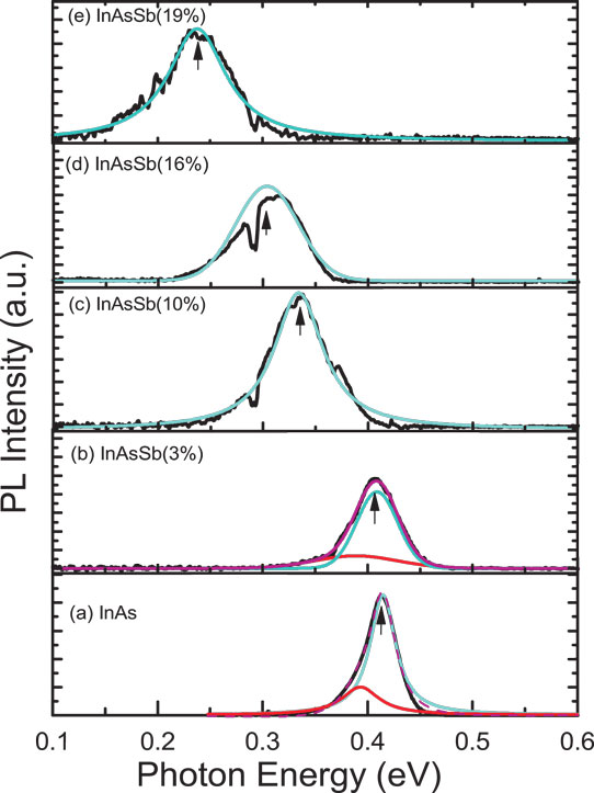
Figure 1: Evolution of 10K photoluminescence of InAs NWs (a) and InAsSb NWs with Sb composition of 3% (b), 10% (c), 16% (d) and 19% (e). Peaks in colors show decomposed emissions.
The low-Sb-content NWs were a mixture of zincblende (ZB) and wurtzite (WZ) crystal structure segments, according to high-resolution transmission electron microscope (TEM) analysis (Figure 2). For 16% Sb content the NWs were predominantly ZB and the 19% NW was pure-ZB.
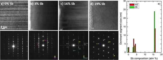
Figure 2: High-resolution TEM images with corresponding fast Fourier electron diffraction patterns of InAs NWs (a) and InAsSb NWs with Sb content of 3% (b), 16% (c), 19% (d), and average size of ZB and WZ segments in InAsSb NWs as a function of Sb content (e).
The researchers believe that increased Sb incorporation could lead to further improved optical properties. They also think that suppressing surface states should also be beneficial. According to the team, surface states are “the major factor impeding the development of NW optoelectronic devices”.
https://doi.org/10.1088/1361-6528/aa59c5
The author Mike Cooke is a freelance technology journalist who has worked in the semiconductor and advanced technology sectors since 1997.


