


- News
10 March 2017
Gallium nitride vertical fin power field-effect transistors with 800V breakdown
Massachusetts Institute of Technology (MIT) has developed a vertical gallium nitride (GaN) fin power field-effect transistor (FET) [Min Sun, et al, IEEE Electron Device Letters, online 17 February 2017]. The device structure avoids the use of material re-growth or of p-GaN layers. Material re-growth increases process complexity and, in a manufacturing context, cost. Layers with p-type GaN tend to have high resistance due to the difficulties of magnesium doping.
The MIT researchers are targeting high-voltage high-current low-cost high-performance power electronics applications. The demonstrated fin power FET with suitable electric field engineering techniques achieved an 800V hard breakdown in the off-state with 0V gate potential.
Lateral GaN devices are now commercially available with 650V breakdown. The MIT team sees the advantages of vertical structures as being:
(1) die area does not depend on breakdown voltage;
(2) the surface is far from high electric field regions, minimizing trapping effects;
(3) high current levels, thanks to easier current extraction when source and drain contacts are positioned vertically on opposite sides of the wafer; and
(4) high thermal performance due to a more widely spread current and electric field distribution.
The epitaxial material was grown using metal-organic chemical vapor deposition (MOCVD) on 2-inch bulk GaN (Figure 1). Submicron fins with 70° sidewalls were etched using inductively coupled plasma (ICP) based on chlorine/boron trichloride chemistry. The dry etch was followed by hot tetramethylammonium hydroxide (TMAH) wet etching to give vertical sidewalls. Alignment of the fins with the <11-20> a-plane of the GaN crystal structure gave smoother fins. The fins were 100μm long and 0.18μm wide.
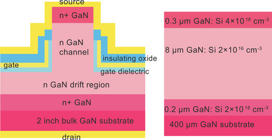
Figure 1: Schematic of vertical fin power FET and starting epi-structure.
The gate consisted of 15nm atomic layer deposition (ALD) of aluminium oxide dielectric and sputtered molybdenum metal electrode. The metal electrode and dielectric were removed from the tops of the fins. Plasma-enhanced chemical vapor deposition (PECVD) silicon dioxide was used as a spacer to isolate the gate metal from the source electrode. The source and backside drain metals were annealed titanium/aluminium.
The on/off current ratio was as high as 1011 with a 5V drain bias (Figure 2). The gate leakage was less than 10-4A/cm2 at a gate-source potential difference of 5V. The threshold voltage for an on/off current ratio of 105 was 1.0V. Based on extrapolation, a higher threshold of 1.5V was found. The researchers comment: “The threshold voltage can shift more positively by reducing the doping density in the channel or scaling down the channel width even further.”
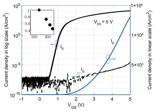
Figure 2: Double sweep transfer curves of fabricated vertical fin power FET with channel width 180nm: left y-axis in log scale; right y-axis in linear scale. Inset: threshold voltage Vth (y-axis, in volts) as a function of channel length (x-axis, in nm).
The subthreshold swing was 75mV/decade and hysteresis effects were small. The on-resistance was 0.36mΩ-cm2 based on fin area and 3.24mΩ-cm2 based on device area. The low annealing temperature of the source-drain electrodes gave imperfect ohmic behavior.
Without edge termination, hard 0V gate off-state breakdown occurred at 100V. A gate field-plate termination structure on silicon dioxide at the device periphery increased breakdown to 400V. “In both cases, the breakdown mechanism is due to gate dielectric failure,” the team reports. Further increase in breakdown voltage to 800V was enabled by filling the trenches of the device with 100nm silicon dioxide before gate formation.
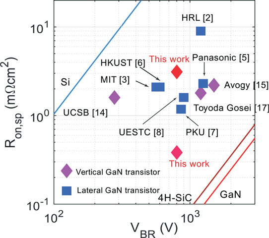
Figure 3: Specific on-resistance (Ron,sp) versus breakdown voltage (VBR) of GaN vertical fin power FET, along with other normally-off lateral and vertical GaN transistors. Top point averaged by total device area and other point averaged by total fin area.
The researchers also present a benchmark comparison with the performance of power transistors produced by other groups (Figure 3).
https://doi.org/10.1109/LED.2017.2670925
The author Mike Cooke is a freelance technology journalist who has worked in the semiconductor and advanced technology sectors since 1997.


