


- News
29 March 2017
Monolithic III-V transistors and laser diodes integrated on germanium
Researchers based in Singapore and USA claim the first monolithic integration of indium gallium arsenide (InGaAs) field-effect transistors (FETs) and electrically pumped InGaAs/GaAs multiple quantum well (MQW) laser diodes on germanium (Ge) substrate using direct epitaxial growth [Annie Kumar et al, Optics Express, vol25, p5146, 2017].
The team from National University of Singapore (NUS) and Nanyang Technological University (NTU) in Singapore and Massachusetts Institute of Technology (MIT) in the USA sees its work as a milestone on the path towards enabling low-power and high-speed optoelectronic integrated circuits (OEICs).
The researchers hope for potential applications in on-chip optical interconnects, giving higher speed, lower interconnect energy, and higher interconnect density than is possible through metal electron conduction.
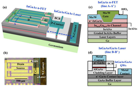
Figure 1: (a) Schematic of monolithic integration of InGaAs n-FETs with lasers. (b) Optical microscope image of optoelectronic integrated circuit with multiple finger InGaAs FETs driving laser.(c) Cross-sectional schematic of fabricated InGaAs FET along line A-A’ in (a). (d) Cross-sectional schematic of fabricated InGaAs/GaAs laser along line B-B’ in (a).
Molecular beam epitaxy (MBE) was carried out on 6°-offcut Ge. The use of germanium substrates reduces lattice mismatch with GaAs, compared with silicon, reducing threading dislocations and defects. The first III-V deposition was 10 monolayers of 300°C migration-enhanced epitaxy (MEE) GaAs. The initial deposition was designed to reduce defects related to anti-phase boundaries in the crystal structure.
Next, 500nm of 580°C n+-GaAs was deposited as the n-contact layer, followed by three GaAs/AlGaAs superlattice layers applied with the aim of suppressing threading dislocations propagating into the laser heterostructure, which began with 1.7μm aluminium gallium arsenide (Al0.4Ga0.6As) bottom cladding.
The MQW active region consisted of three 8nm In0.2Ga0.8As wells and 20nm GaAs barriers. The waveguide region consisted of AlGaAs graded-index separate-confinement heterostructures above and below the MQW with the aluminium content ranging from 0.05 and 0.40. The top cladding was 1.2μm of Al0.4Ga0.6As. The p-contact consisted of 400nm p+-GaAs.
Subsequent transistor layers were a 800nm graded InAlAs buffer with indium content ranging from 0.1 to 0.52, a 15nm In0.53Ga0.47As channel, a 2nm In0.52Al0.48As etch stop, and 30nm of a n+-In0.53Ga0.47As cap. The graded InAlAs buffer was designed to bridge between the lattice constants of the laser and transistors layers.
Transistors were fabricated metal-first with molybdenum source-drain electrodes. Tungsten was used to protect the molybdenum from oxidation during dry etch of the channel region with a silicon dioxide hard mask. After removal of the tungsten and molybdenum, the channel was wet etched down to the 2nm InAlAs stop layer.
The gate stack consisted of 6nm atomic layer deposition (ALD) hafnium dioxide dielectric insulator and sputtered molybdenum and tungsten metal electrode. The gate was patterned and dry etched. Electrical isolation was achieved with a mesa wet etch. The transistor was protected during laser fabrication with a layer of plasma-enhanced chemical vapor deposition (PECVD) silicon dioxide.
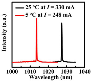 Figure 2: Lasing spectra of diode at 5°C and 25°C.
For the laser diode, the waveguide ridge was wet etched while the facets were formed with dry etch. The n-contact was formed from annealed gold/nickel/gold/germanium/nickel layers. The device was passivated and planarized with benzocyclobutene (BCB). The p-contact metal was gold/titanium.
The researchers report on the low thermal budget silicon CMOS-compatible fabrication: “The highest temperature used in the entire process flow was 400°C to maintain the high quality of QWs and reduce the possible inter-diffusion of the QW layers.”
A 4.5μm-channel nFET had a subthreshold swing of 93mV/decade and an on/off current ratio of more than four orders of magnitude (i.e. 104). The drive current at 1.5V gate potential above threshold (overdrive) was 200μA/μm at 1.5V drain bias.
The capacitance equivalent thickness of the gate insulator was 2nm. A negative impact on the device performance was a large source-drain series resistance of 4.7kΩ-μm, which the researchers believe can be reduced by boosting doping of the n+-InGaAs layer and reducing contact metal sheet resistances.
A device with 21μm-long channel had a peak effective field mobility greater than 2000cm2/V-s, according to split capacitance-voltage measurements. When the inversion carrier density was 1013/cm2, the mobility was 900cm2/V-s.
The laser diode had an on/off current ratio of more than seven orders of magnitude. The lasing threshold current for a 1mmx24μm laser diode was 210mA (875A/cm2) at 5°C, under pulsed operation. The room-temperature threshold was 1.25kA/cm2.
At room temperature, the laser peak wavelength was 1027nm at 330mA injection. This represents a red-shift on photoluminescence emission at 978nm. The researchers suggest that heating during laser operation reduces the bandgap and hence increases the wavelength. The linewidth of the laser peak was 1.7nm. The 5°C measurements gave a short laser wavelength around 1014nm at 248mA with the same linewidth.
InGaAs FETs Electrically pumped InGaAs/GaAs MQW laser diodes Germanium substrate MBE
www.osapublishing.org/oe/abstract.cfm?uri=oe-25-5-5146
The author Mike Cooke is a freelance technology journalist who has worked in the semiconductor and advanced technology sectors since 1997.


