


- News
7 March 2017
Bulk GaN substrate market growing at 10% CAGR to $100m in 2022, from 60,000 wafers in 2016, driven by laser diodes and high-brightness LEDs
Optoelectronics applications, particularly GaN-based laser diodes and GaN-on-GaN LEDs, will drive the bulk gallium nitride (GaN) substrate market from 2016-2022, according to a new report from Yole Développement.
Specific to the laser diode market, the Blu-ray segment, which in the past was the GaN-based laser industry’s main driver, continues to decline. In recent years, a much greater percentage of movies were viewed via streaming than on optical discs, and in many cases flash memory is replacing optical discs and magnetic storage. The current crop of mobile phones, netbooks, tablets, and even laptops lack a Blu-ray/DVD/CD drive. UHD Blu-ray’s recent development is expected to have only a novelty effect on sales - not enough to reverse the general downward trend to be seen in the coming years. However, decreasing Blu-ray demand is expected to be offset by nascent, growing segments like projectors - office projector, mobile pico projector, head-up display (HUD), etc - and automotive lighting, leading to new growth opportunities for bulk GaN substrates.
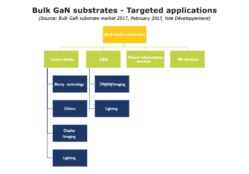
In the LED market, improvements in GaN substrate manufacturing have lowered substrate prices enough for various niche LED applications. In addition to Soraa in the USA and Panasonic in Japan, this seems to have revived the interest of other LED makers that are beginning to seriously consider using GaN substrates for either spotlighting or automotive lighting. New GaN-on-GaN LED players are expected in the market in the coming years.
In this context, Yole expects laser diodes and LEDs to drive continuous growth of bulk GaN substrate demand.
Japanese players dominating market
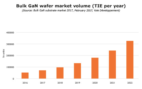
In 2016 the bulk GaN substrate market was estimated to be about 60,000 wafers (two-inch equivalent (TIE)). Essentially all commercial GaN wafers are produced by hydride vapor-phase epitaxy (HVPE) technology, but details of the growth process and separation techniques vary by company. Other techniques, such as Na-flux or Ammonothermal, are still under development. We still don’t see large volume of these wafers on the market. The market is expected to rise at a compound annual growth rate (CAGR) of 10% to more than $100m in 2022.
The GaN substrate market is currently heavily concentrated. More than 85% share is held by three Japanese firms: Sumitomo Electric Industries (SEI), Mitsubishi Chemical Corp (MCC), and Sciocs. Other Japanese and non-Japanese players are still in small-volume production or at the R&D stage, and it is too early for them to challenge these market leaders, says Yole.
GaN-on-GaN technology among different GaN-related technologies
In the past, due to technical complexities, limited availability and the high cost of native bulk GaN substrates for homoepitaxial growth, different foreign substrates were used to develop GaN-based devices for diverse applications:
- GaN-on-sapphire was widely developed, benefiting from the LED industry’s growth over the past 25 years (the first GaN-on-sapphire LEDs hit the market in the 1990s). Sapphire wafer pricing has eroded significantly in the same period, and GaN-on-sapphire remains the dominant technology for LED applications.
- GaN-on-SiC was among the first to be studied. Today the technology is widely used for GaN RF device manufacturing and LED manufacturing.
- GaN-on-silicon arrived naturally, breaking the cost-point and making GaN an affordable technology. However, it faced a host of technical challenges, i.e. high lattice mismatch and high thermal expansion coefficient (TEC) mismatch. Academia and industry have invested heavily to resolve these technical issues, and today GaN-on-silicon is gradually being commercialized, particularly for power electronics applications.
- Many other materials, i.e. polycrystalline AlN substrates, have been proposed as an attractive alternative due to a more closely matched coefficient of thermal expansion (CTE) with GaN. Other more foreign materials (diamond, Ge, and ZnO) have also been studied, but these remain mostly in the R&D stage.
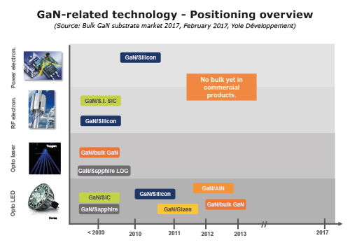
On the other hand, development of bulk GaN substrates was happening in parallel with other substrates. The progress of GaN substrates – specifically, wafer size/quality increase and wafer cost reduction – sees GaN-on-GaN technology entering more and more optoelectronic applications, and possibly electronics applications in the future., reckons Yole.
www.i-micronews.com/compound-semi-report/


