


- News
12 May 2017
Gallium oxide transistor radio-frequency measurements
Researchers in the USA and Germany have claimed the first radio frequency (RF) measurements on β-crystal gallium oxide (β-Ga2O3) metal-oxide-semiconductor field-effect transistors (MOSFETs) [Andrew J. Green et al, IEEE Electron Device Letters, published online 19 April 2017].
The team from Air Force Research Laboratory (AFRL) in the USA, Leibniz Institute for Crystal Growth in Germany, and George Mason University and KBRwyle in the USA further claim record-high transconductance and frequency characteristics. “The RF result is achieved through the reduction of contact resistance, due to a highly doped cap layer, and through the use of a gate recess, allowing for gate length scaling,” the researchers comment.
The team believes that the MOSFETs point the way to monolithic or heterogeneous integration of power switch and other RF devices on β-Ga2O3. Such devices benefit from the ultra-wide 5eV bandgap that theory suggests could lead to critical fields for breakdown as high as 8MV/cm. The breakdown fields for gallium nitride (3.4eV bandgap) and silicon carbide (~3eV) are up to 5MV/cm. Greater critical fields should lead to higher breakdown voltages in devices.
The team comments: “These early results indicate promising RF potential for β-Ga2O3 MOSFETs as crystallinity improves and device scaling techniques are implemented. Additionally, dramatic improvements are expected with heterostructure development.”
The device material was grown by metal-organic vapor phase epitaxy (MOVPE) on 2-inch semi-insulating (100) β-Ga2O3. The wafer was offcut 6° from the (100) plane to encourage step-flow growth, reducing planar defects. The epitaxial layers were silicon doped with 1x10¹⁸/cm3 concentration for 180nm and 1x10¹⁹/cm3 for 25nm to give the channel and ohmic contact, respectively.
Device fabrication began with mesa isolation etch with boron trichloride inductively coupled plasma. The ohmic source and drain contacts were evaporated and annealed titanium/aluminium/nickel/gold.
Gate formation began with boron trichloride inductively coupled plasma reactive-ion etch to expose the channel layer. The device was then coated with 200nm silicon dioxide (SiO2) for passivation and for field-plate separation. The SiO2 was etched to give a 0.7μm-wide gate trench. The etch was continued ~90nm into the channel layer to give a gate recess.
The gate dielectric was 20nm atomic layer deposition (ALD) aluminium oxide (Al2O3). Nickel/gold was used for local interconnection and gate electrodes. Extra current handling was enabled by the use of 2μm-thick titanium/gold interconnections.
Hall-effect measurements using van der Pauw structures on post-processed material with the ohmic cap layer removed gave a carrier concentration of 1.3x10¹⁸/cm3 and 96cm2/V-s mobility. Transfer length measurements gave contact resistance of 3.3Ω-mm and 4850Ω/square sheet resistance.
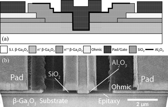
Figure 1: (a) Cross-sectional schematic for β-Ga2O3 MOSFET. (b) Focused ion beam cross-sectional image showing bottom finger of 2x50μm split finger gate.
The final MOSFETs (Figure 1) had a 3.8μm source-drain spacing. The gate-drain distance was 1.6μm.
The devices achieved an on/off current ratio of 106 and 150mA/mm maximum drain current at 40V drain bias and 0V gate potential. The threshold voltage was estimated at -10.1V through linear extrapolation of the transconductance curve.
The peak transconductance was 21.2mS/mm. The researchers claim that this is 7x the group’s previously reported β-Ga2O3 MOSFET performance and is also “higher than any other published result for β-Ga2O3”.
With the drain biased at 40V and the gate potential at -3.5V (the position of the peak transconductance), the small-signal cut-off frequency (fT) was 2.7GHz and the maximum oscillation (fmax) was 12.9GHz. Varying the drain bias allowed fT to reach 3.3GHz. By contrast, the highest fmax occurred at 40V, after saturation at 35V.
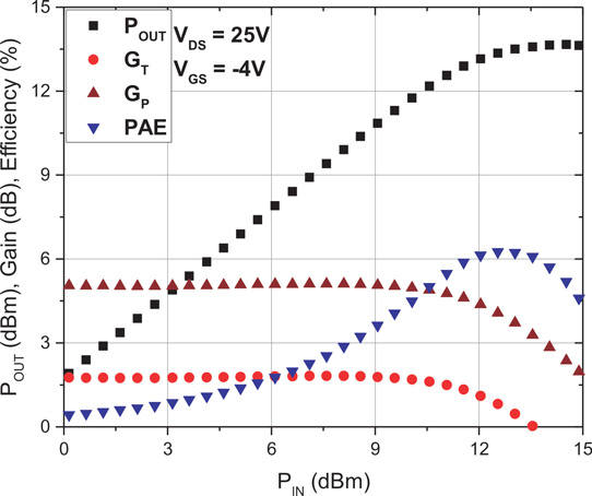
Figure 2: 800MHz Class-A power sweep of a 2x50 μm β-Ga2O3 gate recessed MOSFET.
Large-signal continuous-wave 800MHz performance was also measured with 25V drain bias and -4V gate potential (see Figure 2). A passive source was used with load tuning for maximum output power, giving approximate Class A operation. The output power reached 0.23mW/mm (13.7dBm).
The team reports: “Both small- and large-signal measurements had significant reflected power due to a large high input impedance (small device periphery of 100μm coupled with a large sheet resistance of 4850Ω/□) of the device which could not be properly matched at the source side.”
The effect was measured and corrected for by suitably reducing the input power value to give maximum transducer and power gain figures of 1.8dB and 5.1dB, respectively. The maximum power-added efficiency (PAE) was 6.3%.
Increasing the drain bias to 50V gave an output power of 0.25W/mm, but a low power-added efficiency of 1.4%. Catastrophic failure occurred for this high bias with the operating temperature reaching 300°C due to self-heating thermal effects, degrading device performance.
https://doi.org/10.1109/LED.2017.2694805
The author Mike Cooke is a freelance technology journalist who has worked in the semiconductor and advanced technology sectors since 1997.


